onsemi MC74AC373
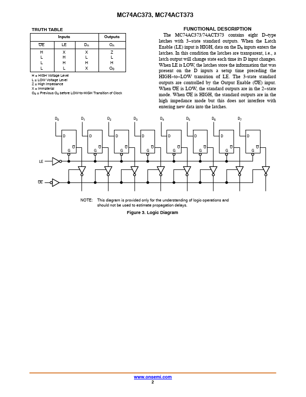
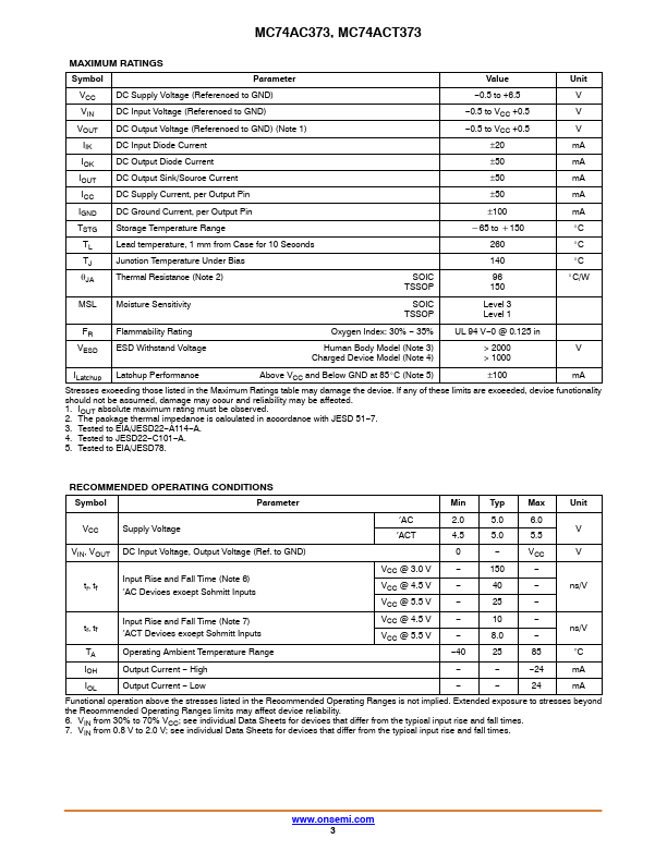
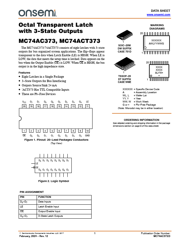
The MC74AC373/74ACT373 consists of eight latches with 3−state outputs for bus organized system applications. The flip−flops appear transparent to the data when Latch Enable (LE) is HIGH. When LE is LOW, the data that meets the setup time is latched.| Part No. | MC74AC373 |
|---|---|
| Datasheet | MC74AC373 Download |
| Manufacturer |  onsemi |
| Description | Octal Transparent Latch |
| Buy | Stock & Price |
FEATURES
● Eight Latches in a Single Package● 3−State Outputs for Bus Interfacing
● Outputs Source/Sink 24 mA
● ′ACT373 Has TTL Compatible Inputs
● These are Pb−Free Devices VCC O7 D7 D6 O6 O5 D5 D4 O4 LE 20 19 18 17 16 15 14 13 12 11 DATA SHEET 1 SOIC−20W DW SUFFIX CASE 751D MARKING DIAGRAMS 20 XXXXXX AWLYYWWG 1 1 TSSOP−20 DT SUFFIX CASE 948E 20 XXXX XXXX ALYWG G 1 XXXXXX = Specific Device Code A = Assembly Location WL, L = Wafer Lot YY, Y = Year WW, W = Work Week G or G = Pb−Free Package (Note: Microdot may be in either location) 1 2 3 4 5 6 7 8 9 10 OE O0 D0 D1 O1 O2 D2 D3 O3 GND Figure 1. Pinout: 20−Lead Packages Conductors (Top View) ORDERING INFORMATION See detailed ordering and shipping information in the package dimensions section on page 8 of this data sheet. D0 D1 D2 D3 D4 D5 D6 D7 LE OE O0 O1 O2 O3 O4 O5 O6 O7 Figure 2. Logic Symbol PIN ASSIGNMENT PIN FUNCTION D0−D7 LE Data Inputs Latch Enable Input OE Output Enable Input O0−O7 3−State Latch Outputs © Semiconductor Components Industries, LLC, 2017 1 February, 2024 − Rev.