onsemi MC74ACT299
The MC74AC299/74ACT299 is an 8−bit universal shift/storage register with 3−state outputs. The parallel load inputs and flip−flop outputs are multiplexed to reduce the total number of package pins.| Part No. | MC74ACT299 |
|---|---|
| Datasheet | MC74ACT299 Download |
| Manufacturer |  onsemi |
| Description | 8-Input Universal Shift/Storage Register |
| Buy | Stock & Price |
APPLICATIONS
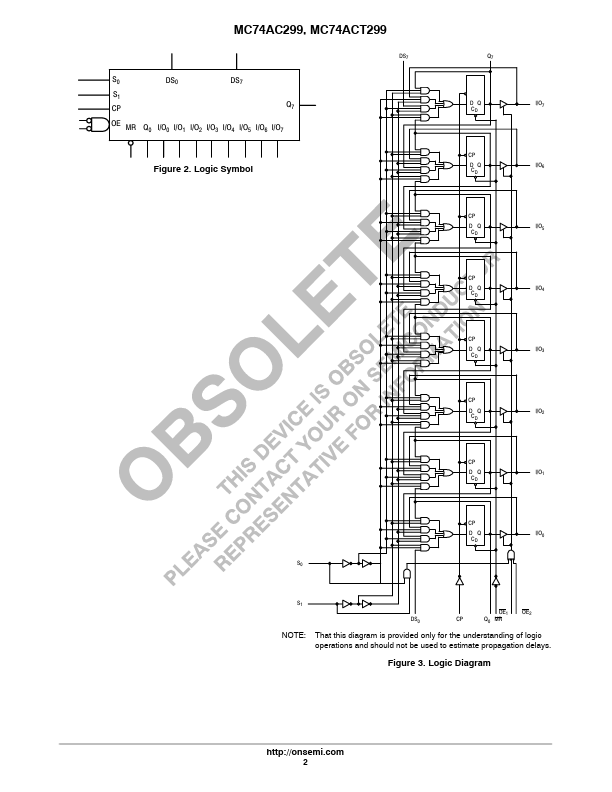
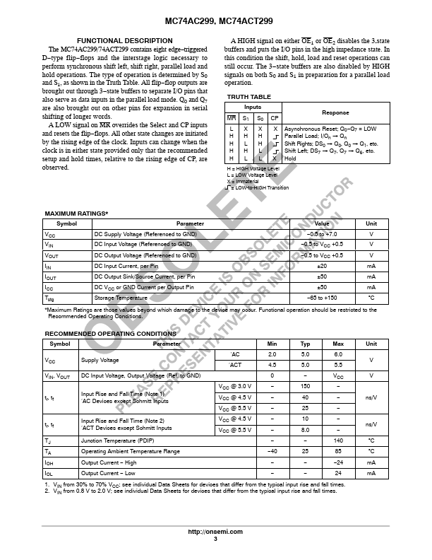
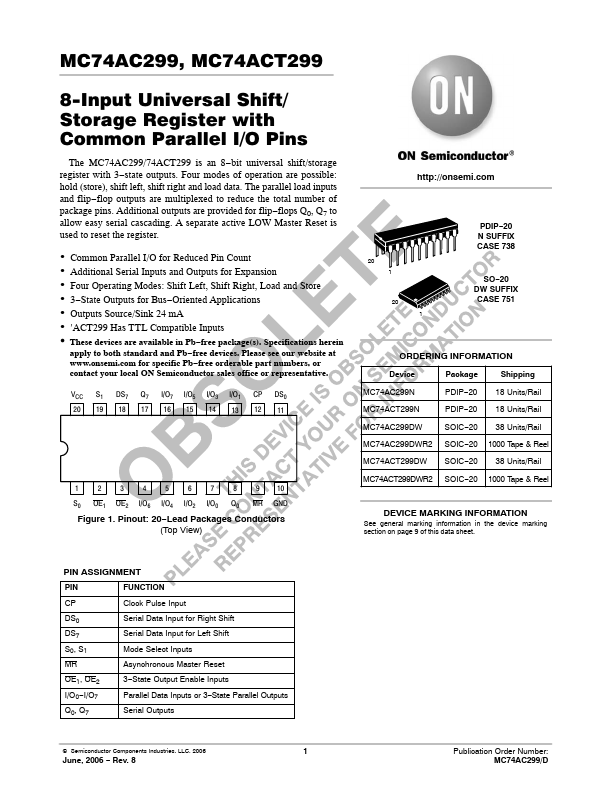
● Outputs Source/Sink 24 mA● ′ACT299 Has TTL Compatible Inputs w These devices are available in Pb−free package(s). Specifications herein apply to both standard and Pb−free devices. Please see our website at for specific Pb−free orderable part numbers, or contact your local ON Semiconductor sales office or representative. VCC S1 DS7 Q7 I/O7 I/O5 I/O3 I/O1 CP DS0 20 19 18 17 16 15 14 13 12 11 1 2 3 4 5 6 7 8 9 10 S0 OE1 OE2 I/O6 I/O4 I/O2 I/O0 Q0 MR GND Figure 1. Pinout: 20−Lead Packages Conductors (Top View) 20 1 20 1 PDIP−20 N SUFFIX CASE 738 SO−20 DW SUFFIX CASE 751 ORDERING INFORMATION Device Package Shipping MC74AC299N PDIP−20 18 Units/Rail MC74ACT299N PDIP−20 18 Units/Rail MC74AC299DW SOIC−20 38 Units/Rail MC74AC299DWR2 SOIC−20 1000 Tape & Reel MC74ACT299DW SOIC−20 38 Units/Rail MC74ACT299DWR2 SOIC−20 1000 Tape & Reel DEVICE MARKING INFORMATION See general marking information in the device marking section on page 9 of this data sheet. PIN ASSIGNMENT PIN FUNCTION CP C...