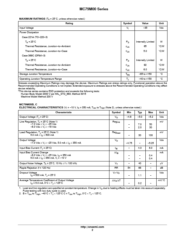
MAXIMUM RATINGS
(TA = 25°C, unless otherwise noted.) Rating Input Voltage Power Dissipation Case 221A TA = 25°C Thermal Resistance, Junction–to–Ambient Thermal Resistance, Junction–to–Case Case 369 and 369A (DPAK) TA = 25°C Thermal Resistance, Junction–to–Ambient Thermal Resistance, Junction–to–Case Storage Junction Temperature Junction Temperature NOTE: ESD data available upon request. Symbol VI Value –35 Unit Vdc PD θJA θJC PD θJA θJC Tstg TJ Internally Limited 65 5.0 Internally Limited 92 6.0 –65 to +150 150 W °C/W °C/W W °C/W °C/W °C °C THERMAL CHARACTERISTICS Characteristic Thermal Resistance, Junction–to–Ambient Thermal Resistance, Junction–to–Case Symbol RθJA RθJC Value 65 5.0 Unit °C/W °C/W MC79M05B, C ELECTRICAL CHARACTERISTICS
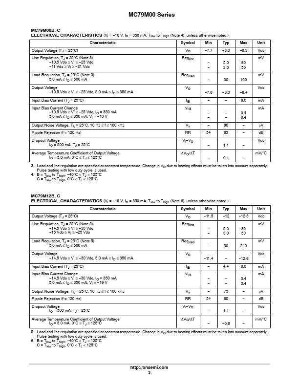
(VI = –10 V, IO = 350 mA, Tlow to Thigh [Note 2], unless otherwise noted.) Characteristic Output Voltage (TJ = 25°C) Line Regulation, TJ = 25°C (Note 1) –7.0 Vdc ≥ VI ≥ –25 Vdc –8.0 Vdc ≥ VI ≥ –18 Vdc Load Regulation, TJ = 25°C (Note 1) 5.0 mA ≤ IO ≤ 50... onsemi