onsemi MJE13009G
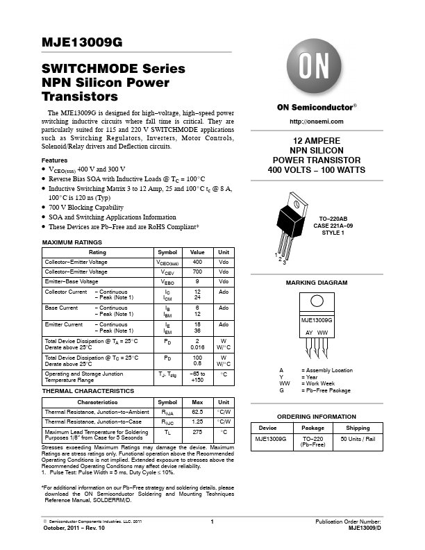
The MJE13009G is designed for high−voltage, high−speed power switching inductive circuits where fall time is critical. They are particularly suited for 115 and 220 V SWITCHMODE applications such as Switching Regulators, Inverters, Motor Controls, Solenoid/Relay drivers and Deflection circuits.| Part No. | MJE13009G |
|---|---|
| Datasheet | MJE13009G Download |
| Manufacturer |  onsemi |
| Description | NPN Silicon Power Transistors |
| Buy | Stock & Price |
FEATURES
● VCEO(sus) 400 V and 300 V● Reverse Bias SOA with Inductive Loads @ TC = 100_C
● Inductive Switching Matrix 3 to 12 Amp, 25 and 100_C tc @ 8 A, 100_C is 120 ns (Typ)
● 700 V Blocking Capability
● SOA and Switching
APPLICATIONS
Information● These Devices are Pb−Free and are RoHS Compliant*
MAXIMUM RATINGS
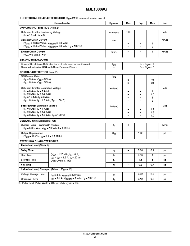
Rating Collector−Emitter Voltage Collector−Emitter Voltage Emitter−Base Voltage Collector Current − Continuous − Peak (Note 1) Base Current − Continuous − Peak (Note 1) Emitter Current − Continuous − Peak (Note 1) Total Device Dissipation Derate above 25°C @ TA = 25_C Total Device Dissipation @ TC = 25_C Derate above 25°C Operating and Storage Junction Temperature Range Symbol VCEO(sus) VCEV VEBO IC ICM IB IBM IE IEM PD PD TJ, Tstg Value 400 700 9 12 24 6 12 18 36 2 0.016 100 0.8 −65 to +150 Unit Vdc Vdc Vdc Adc Adc Adc W W/_C W W/_C _C THERMAL CHARACTERISTICS Characteristics Symbol Max Unit Thermal Resistance, Junction−to−Ambient Thermal Resistance, Junction−to−Case Maximu...