onsemi MMBD1010LT1
Switching Diode
| Part No. | MMBD1010LT1 |
|---|---|
| Datasheet | MMBD1010LT1 Download |
| Manufacturer |  onsemi |
| Description | Switching Diode |
| Buy | Stock & Price |
APPLICATIONS
● ESD Protection● Reverse Polarity Protection
● Steering Logic
● Medium−Speed Switching
MAXIMUM RATINGS
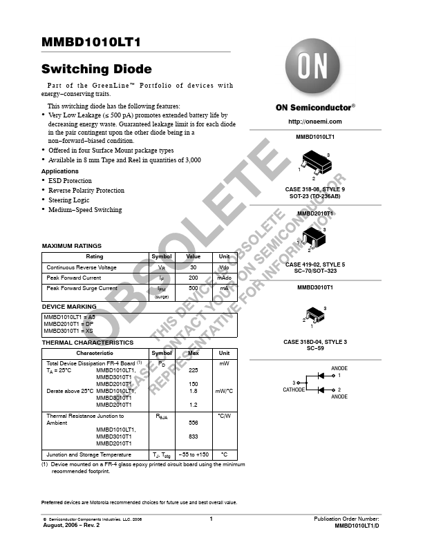
Rating Symbol Value Unit Continuous Reverse Voltage Peak Forward Current Peak Forward Surge Current DEVICE MARKING VR 30 Vdc IF 200 mAdc IFM (surge) 500 mA MMBD1010LT1 = A5 MMBD2010T1 = DP MMBD3010T1 = XS THERMAL CHARACTERISTICS Characteristic Total Device Dissipation FR-4 Board (1) TA = 25°C MMBD1010LT1, MMBD3010T1 MMBD2010T1 Derate above 25°C MMBD1010LT1, MMBD3010T1 MMBD2010T1 Symbol PD Max 225 150 1.8 1.2 Unit mW mW/°C Thermal Resistance Junction to Ambient MMBD1010LT1, MMBD3010T1 MMBD2010T1 RθJA °C/W 556 833 Junction and Storage Temperature TJ, Tstg − 55 to +150 °C (1) Device mounted on a FR-4 glass epoxy printed circuit board using the minimum recommended footprint. Preferred devices are Motorola recommended choices for future use and best overall value. © Semiconductor Components Industries, LLC, 2006 August, 2006 − Rev. 2 1 MMBD1010LT1 3 1 2 CASE 318-08, STYLE 9...