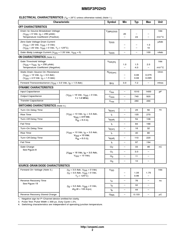
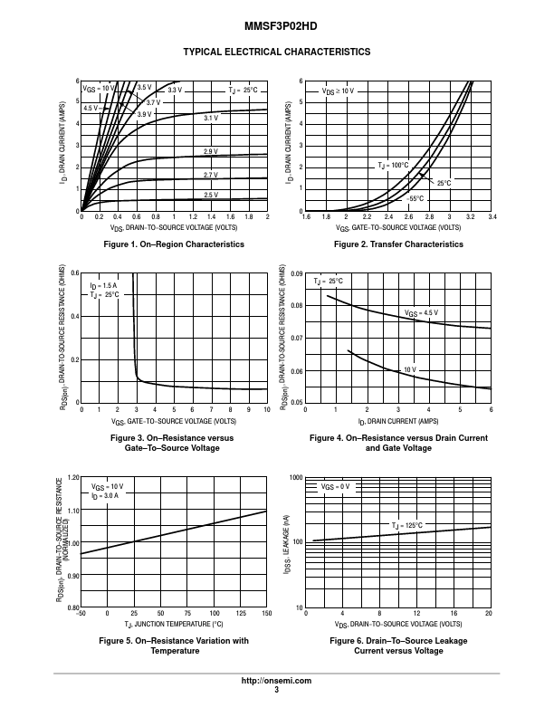
onsemi MMSF3P02HD
Power MOSFET
| Part No. | MMSF3P02HD |
|---|---|
| Datasheet | MMSF3P02HD Download |
| Manufacturer |  onsemi |
| Description | Power MOSFET |
| Buy | Stock & Price |
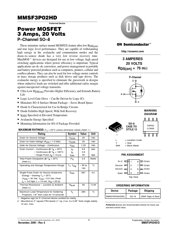
MAXIMUM RATINGS
(TJ = 25°C unless otherwise noted) (Note 1.) Rating Symbol Value Unit Drain–to–Source Voltage Drain–to–Gate Voltage (RGS = 1.0 MΩ) Gate–to–Source Voltage – Continuous Drain Current – Continuous @ TA = 25°C Drain Current – Continuous @ TA = 100°C Drain Current – Single Pulse (tp ≤ 10 µs) Total Power Dissipation @ TA = 25°C (Note 2.) VDSS VDGR VGS ID ID IDM PD 20 Vdc 20 Vdc ± 20 Vdc 5.6 Adc 3.6 30 Apk 2.5 Watts Operating and Storage Temperature Range TJ, Tstg – 55 to 150 °C Single Pulse Drain–to–Source Avalanche Energy – Starting TJ = 25°C (VDD = 20 Vdc, VGS = 5.0 Vdc, Peak IL = 9.0 Apk, L = 14 mH, RG = 25 Ω) Thermal Resistance – Junction to Ambient (Note 2.) EAS RθJA 567 mJ 50 °C/W Maximum Lead Temperature for Soldering Purposes, 1/8″ from case for 10 seconds TL 260 °C 1. Negative sign for P–Channel device omitted for clarity. 2. Mounted on 2″ square FR4 board (1″ sq. 2 oz. Cu 0.06″ thick single sided), 10 sec. max. 3 AMPERES 20 VOLTS RDS(on) = 75 mW P–Channel D G S MARK...