onsemi NB3N508S
The NB3N508S is a high precision, low phase noise Voltage Controlled Crystal Oscillator (VCXO) and phase lock loop (PLL) that generates 216 MHz M−LVDS output from a 27 MHz crystal. The ±100 ppm output pullable range is obtained using the VIN pin of the VCXO with usable range from 0 V to 3.3 V. The VCXO input pin VIN is a high−impedance input that can be driven directly from a pulse width modulated RC integrator circuit.- Min Voltage : 3.135V
- Max Voltage : 3.465V
- Max Operating Temp : 70°C
- Min Operating Temp : 0°C
Source:
Octopart
| Part No. | NB3N508S |
|---|---|
| Datasheet | NB3N508S Download |
| Manufacturer |  onsemi |
| Description | PureEdge VCXO Clock Generator |
| Buy | Stock & Price |
DESCRIPTION
The NB3N508S is designed primarily for data and clock recovery applications within end products such as ADSL modems, set−top box receivers, and telecom systems. This device is housed in 5.0 mm x 4.4 mm narrow body TSSOP−16 pin package.FEATURES
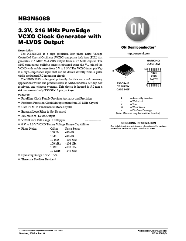
MARKING DIAGRAM 16 1 TSSOP−16 DT SUFFIX CASE 948F 1 16 NB3N 508S ALYWG G●
●
●
●
●
●
●
●
●
● PureEdge Clock Family Provides Accuracy and Precision Performs Precision Clock Multiplication from 27 MHz Crystal Uses 27 MHz Fundamental Mode Crystal External Loop Filter is Not Required 216 MHz M−LVDS Output VCXO with Pull Range $100 ppm 0 V to 3.3 V VCXO Tuning Voltage Range Capabilities Phase Noise: Offset Noise Power 100 Hz −80 dBc 1 kHz −88 dBc 10 kHz −105 dBc 100 kHz −106 dBc 1 MHz −120 dBc 10 MHz −145 dBc Operating Range 3.3 V $5% These are Pb−Free Devices* A = Assembly Location L = Wafer Lot Y = Year W = Work Week G = Pb−Free Package (Note: Microdot may be in either location) ORDERING INFORMATION See detailed ordering and shipping information in the package dimensions section on page 7 of this data sheet. © Semiconductor Components Industries, LLC, 2006 October, 2006 − Rev.

