onsemi NB4L7210
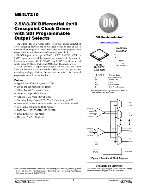
The NB4L7210 is a Clock input crosspoint fanout distribution device selecting between one of two input clocks on each of the 10 differential output pairs.| Part No. | NB4L7210 |
|---|---|
| Datasheet | NB4L7210 Download |
| Manufacturer |  onsemi |
| Description | 2.5V/3.3V Differential 2x10 Crosspoint Clock Driver |
| Buy | Stock & Price |
FEATURES
● Typical Input Clock Frequency > 2 GHz● 200 ps Typical Rise and Fall Times
● 800 ps Typical Propagation Delay
● Output to Output Skew 150 ps
● Additive RMS Phase Jitter of 0.2 ps
● Operating Range: VCC = 2.375 V to 3.6 V with VEE = 0 V
● Differential LVPECL Output Level (Typ 700 mV Peak−to−Peak)
● Low Profile 8x8 mm, 52 QFN Package
● 10GE WAN: 155.52 MHz / 622.08 MHz
● 10GE LAN: 161.1328 MHz
● These are Pb−Free Devices* 1 52 QFN52 MN SUFFIX CASE 485M MARKING DIAGRAM* 52 1 NB4L 7210 AWLYYWWG NB4L7210 A WL YY WW G = Device Code = Assembly Site = Wafer Lot = Year = Work Week = Pb−Free Package *For additional marking information, refer to Application Note AND8002/D. VTCLK0 CLK0 CLK0b VTCLK0b Q0 Q0b Q1 Q1b VTCLK1 CLK1 CLK1b VTCLK1b VCC VEE SCLK SDATA SLOAD Q8 Q8b Q9 Q9b SDATAOUT Figure 1. Functional Block Diagram *For additional information on our Pb−Free strategy and soldering details, please download the ON Semiconductor Soldering and Mounting Techniques Reference Manual, SOLDERRM/D.