DESCRIPTION
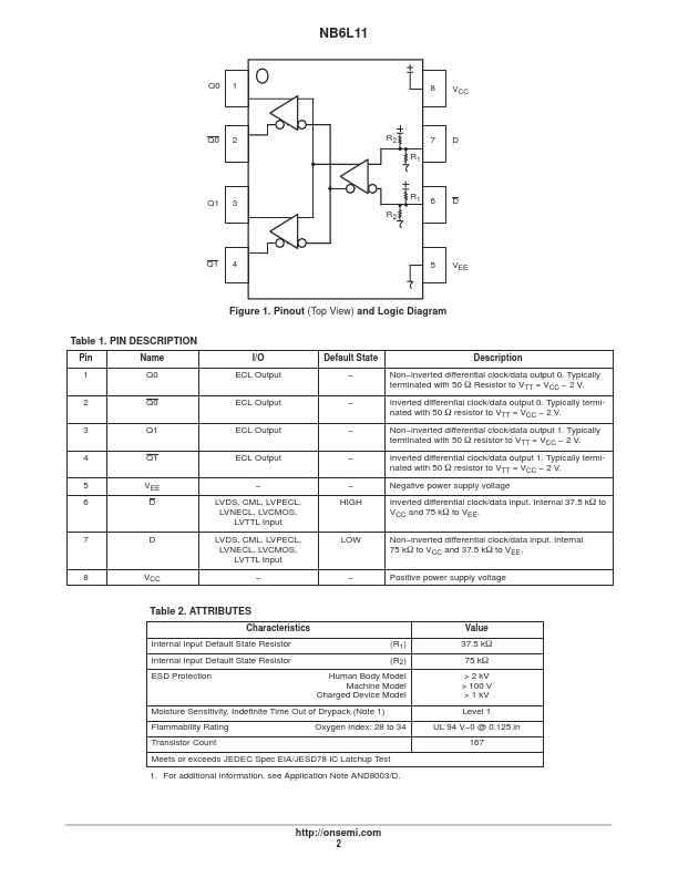
Pin 1 2 3 4 5 6 Name Q0 Q0 Q1 Q1 VEE D ÁÁÁÁ ÁÁÁÁÁÁ ÁÁÁÁÁÁÁÁ ÁÁÁÁ ÁÁÁÁÁÁ ÁÁÁÁÁÁÁÁ ÁÁÁÁ ÁÁÁÁÁÁ ÁÁÁÁÁÁÁÁ I/O ECL Output ECL Output ECL Output ECL Output − LVDS, CML, LVPECL, LVNECL, LVCMOS, LVTTL Input LVDS, CML, LVPECL, LVNECL, LVCMOS, LVTTL Input − Default State − − − − − HIGH ÁÁÁÁÁÁÁÁÁÁÁÁÁÁ ÁÁÁÁÁÁÁÁÁÁÁÁÁÁ ÁÁÁÁÁÁÁÁÁÁÁÁÁÁ DESCRIPTION
Non−inverted differential clock/data output 0. Typically terminated with 50 W Resistor to VTT = VCC − 2 V. Inverted differential clock/data output 0. Typically terminated with 50 W resistor to VTT = VCC − 2 V. Non−inverted differential clock/data output 1. Typically terminated with 50 W resistor to VTT = VCC − 2 V. Inverted differential clock/data output 1. Typically terminated with 50 W resistor to VTT = VCC − 2 V. Negative power supply voltage Inverted differential clock/data input. Internal 37.5 kW to VCC and 75 kW to VEE. Non−inverted differential clock/data input. Internal 75 kW to VCC and 37.5 kW to VEE. Positive power supply voltage 7 D LOW 8 VCC − Table 2. onsemi