onsemi NB6L56
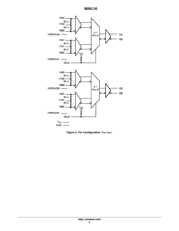
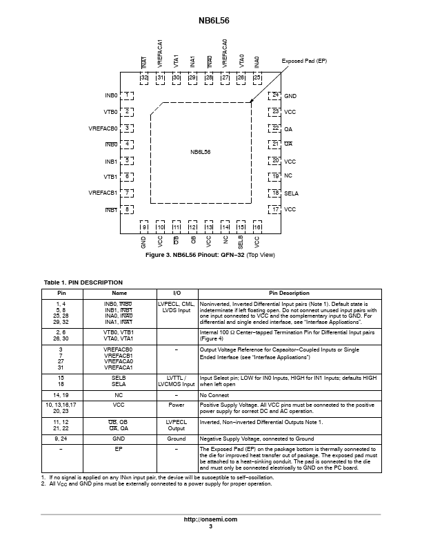
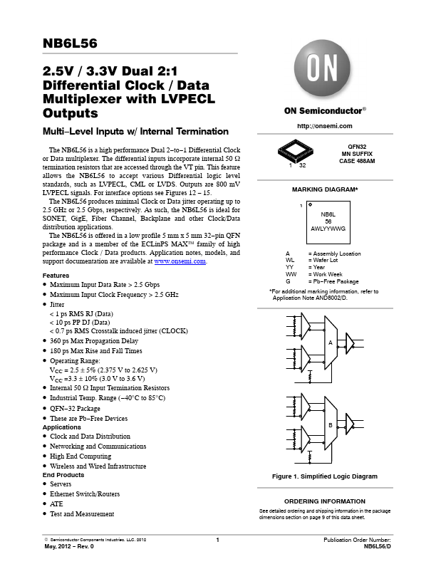
The NB6L56 is a high performance Dual 2−to−1 Differential Clock or Data multiplexer. The differential inputs incorporate internal 50 W termination resistors that are accessed through the VT pin. This feature allows the NB6L56 to accept various Differential logic level standards, such as LVPECL, CML or LVDS.| Part No. | NB6L56 |
|---|---|
| Datasheet | NB6L56 Download |
| Manufacturer |  onsemi |
| Description | 2.5V / 3.3V Dual 2:1 Differential Clock / Data Multiplexer |
| Buy | Stock & Price |
FEATURES
● Maximum Input Data Rate > 2.5 Gbps● Maximum Input Clock Frequency > 2.5 GHz
● Jitter < 1 ps RMS RJ (Data) < 10 ps PP DJ (Data) < 0.7 ps RMS Crosstalk induced jitter (CLOCK)
● 360 ps Max Propagation Delay
● 180 ps Max Rise and Fall Times
● Operating Range: VCC = 2.5 ± 5% (2.375 V to 2.625 V) VCC =3.3 ± 10% (3.0 V to 3.6 V)
● Internal 50 W Input Termination Resistors
● Industrial Temp. Range (−40°C to 85°C)
● QFN−32 Package
● These are Pb−Free Devices
APPLICATIONS
● Clock and Data Distribution● Networking and Communications
● High End Computing
● Wireless and Wired Infrastructure End Products
● Servers
● Ethernet Switch/Routers
● ATE
● Test and Measurement 1 32 QFN32 MN SUFFIX CASE 488AM MARKING DIAGRAM* 1 NB6L 56 AWLYYWWG A = Assembly Location WL = Wafer Lot YY = Year WW = Work Week G = Pb−Free Package *For additional marking information, refer to Application Note AND8002/D. A B Figure 1. Simplified Logic Diagram ORDERING INFORMATION See detailed ordering and shipping information in the package dimensions section on page 9 of this data sheet. © Semiconductor Components Industries, LLC, 2012 May, 2012 − Rev.