DESCRIPTION
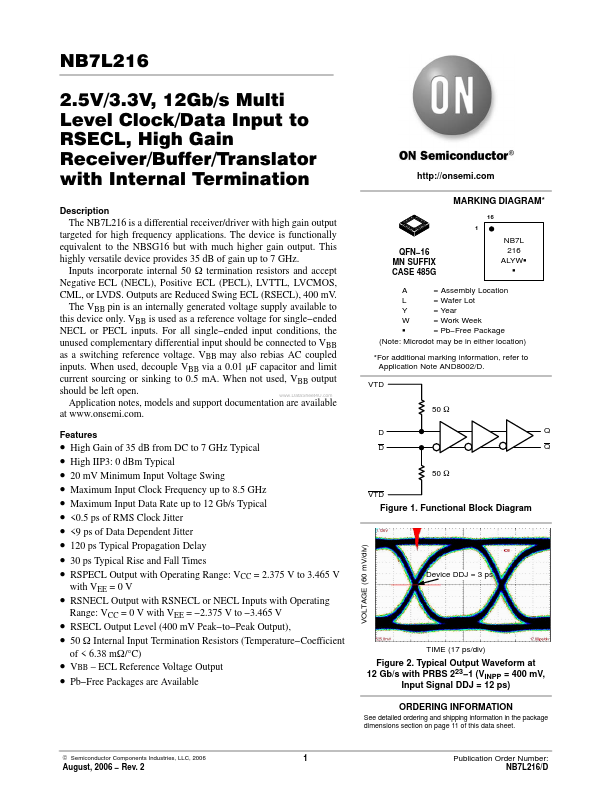
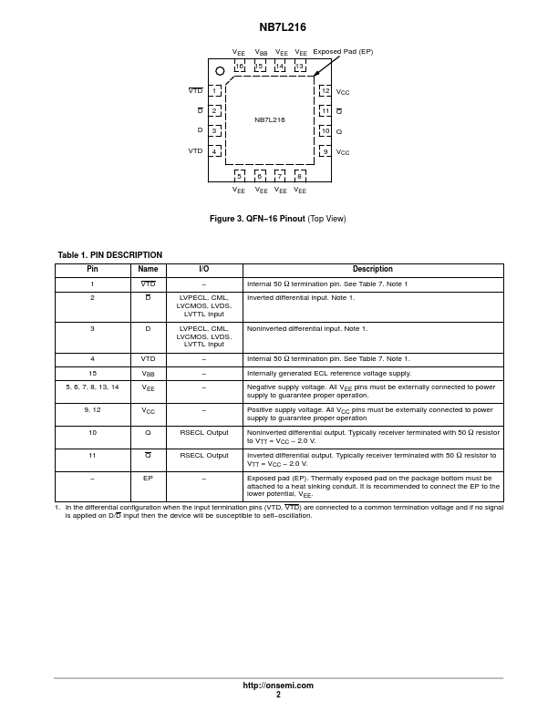
MARKING DIAGRAM* Inputs incorporate internal 50 W termination resistors and accept Negative ECL (NECL), Positive ECL (PECL), LVTTL, LVCMOS, CML, or LVDS. Outputs are Reduced Swing ECL (RSECL), 400 mV. The VBB pin is an internally generated voltage supply available to this device only. VBB is used as a reference voltage for single−ended NECL or PECL inputs. For all single−ended input conditions, the unused complementary differential input should be connected to VBB as a switching reference voltage. VBB may also rebias AC coupled inputs. When used, decouple VBB via a 0.01 mF capacitor and limit current sourcing or sinking to 0.5 mA. When not used, VBB output should be left open. Application notes, models and support documentation are available at FEATURES
16 1 QFN−16 MN SUFFIX CASE 485G NB7L 216 ALYWG G A = Assembly Location L = Wafer Lot Y = Year W = Work Week G = Pb−Free Package (Note: Microdot may be in either location) *For additional marking information, refer to Application Note AND8002/D. onsemi