DESCRIPTION
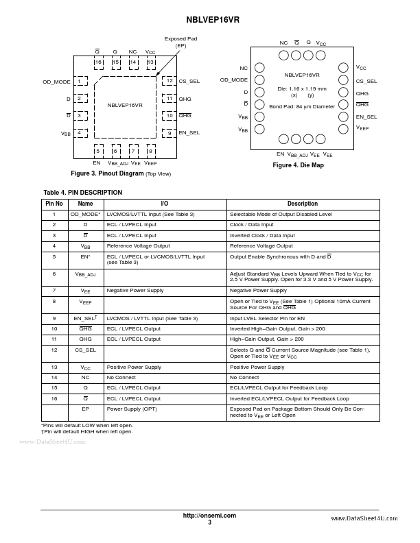
Pin No 1 2 3 4 5 6 7 8 9 10 11 12 13 14 15 16 Name OD_MODE* D D VBB EN* VBB_ADJ VEE VEEP EN_SEL† QHG QHG CS_SEL VCC NC Q Q EP Positive Power Supply No Connect ECL / LVPECL Output ECL / LVPECL Output Power Supply (OPT) LVCMOS / LVTTL Input (See Table 3) ECL / LVPECL Output ECL / LVPECL Output Negative Power Supply I/O LVCMOS/LVTTL Input (See Table 3) ECL / LVPECL Input ECL / LVPECL Input Reference Voltage Output ECL / LVPECL or LVCMOS/LVTTL Input (see Table 3) DESCRIPTION
Selectable Mode of Output Disabled Level Clock / Data Input Inverted Clock / Data Input Reference Voltage Output Output Enable Synchronous with D and D Adjust Standard VBB Levels Upward When Tied to VCC for 2.5 V Power Supply. Open for 3.3 V and 5 V Power Supply. Negative Power Supply Open or Tied to VEE (See Table 1) Optional 10mA Current Source For QHG and QHG Input LVEL Selector Pin for EN Inverted High−Gain Output, Gain > 200 High−Gain Output, Gain > 200 Selects Q and Q Current Source Magnitude (see Tab... onsemi