onsemi NCP1729
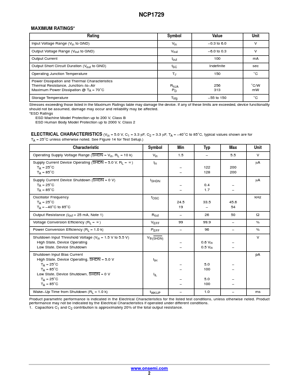
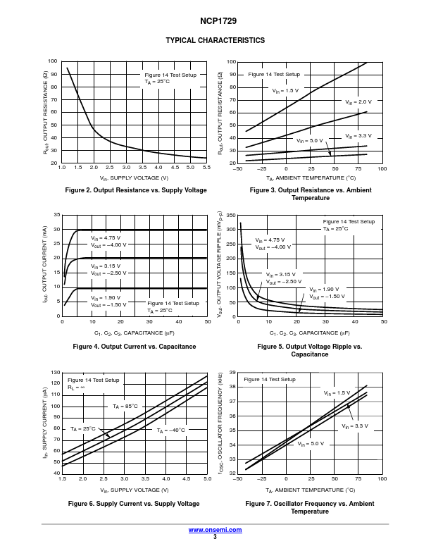
The NCP1729 is a CMOS charge pump voltage inverter that is designed for operation over an input voltage range of 1.5 V to 5.5 V with an output current capability in excess of 50 mA. The operating current consumption is only 122 mA, and a power saving shutdown input is provided to further reduce the current to a mere 0.4 mA. The device contains a 35 kHz oscillator that drives four low resistance MOSFET switches, yielding a low output resistance of 26 W and a voltage conversion efficiency of 99%.- Min Voltage : 1.5V
- Max Voltage : 5.5V
- Max Operating Temp : 85°C
- Min Operating Temp : -40°C
Source:
Octopart
| Part No. | NCP1729 |
|---|---|
| Datasheet | NCP1729 Download |
| Manufacturer |  onsemi |
| Description | Switched Capacitor Voltage Inverter |
| Buy | Stock & Price |
FEATURES
● Operating Voltage Range of 1.5 V to 5.5 V● Output Current Capability in Excess of 50 mA
● Low Current Consumption of 122 mA
● Power Saving Shutdown Input for a Reduced Current of 0.4 mA
● Operation at 35 kHz
● Low Output Resistance of 26 W
● Space Saving TSOP−6 Package
● NCV Prefix for Automotive and Other
APPLICATIONS
Requiring Unique Site and Control Change Requirements; AEC−Q100 Qualified and PPAP Capable● These Devices are Pb−Free and are RoHS Compliant Typical
APPLICATIONS
● LCD Panel Bias● Cellular Telephones
● Pagers
● Personal Digital Assistants
● Electronic Games
● Digital Cameras
● Camcorders
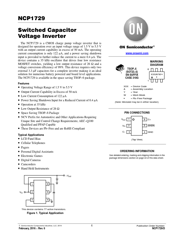
● Hand Held Instruments −Vout 16 Vin 2 3 5 4 TSOP−6 1 (SOT23−6) SN SUFFIX CASE 318G MARKING DIAGRAM 6 XXXAYW G G 1 XXX A Y W G = Device Code = Assembly Location = Year = Work Week = Pb−Free Package (Note: Microdot may be in either location) PIN CONNECTIONS Vout 1 Vin 2 C− 3 6 C+ 5 SHDN 4 GND (Top View) ORDERING INFORMATION See detailed ordering, marking and shipping information in the package dimensions section on page 22 of this data sheet.