onsemi NCP459
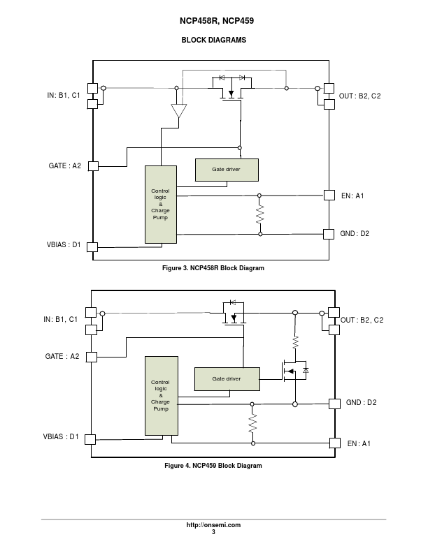
the NCP459 version , to eliminate residual voltages on the external components connected on output pin. NCP458R, NCP459 4 A Single Load Switch for Low Voltage Rail The NCP458R and NCP459 are power load switch with very low Ron NMOSFET controlled by external logic pin, allowing optimization of battery life, and portable device autonomy.| Part No. | NCP459 |
|---|---|
| Datasheet | NCP459 Download |
| Manufacturer |  onsemi |
| Description | 4A Single Load Switch |
| Buy | Stock & Price |
FEATURES
● 0.75 V − 5.5 V Operating Range● 11 mW N−MOSFET
● Vbias Rail Input
● DC Current up to 4 A
● Output Auto−Discharge Option
● Reverse Blocking Option
● Active High EN Pin
● CSP8, 1 x 2 mm2, Pitch 0.5 mm Typical
APPLICATIONS
● Notebooks● Tablets
● Wireless
● Mobile Phones
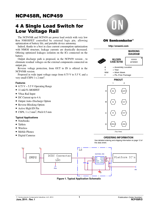
● Digital Cameras Vcc V+ SMPS DCDC Converter or LDO LS MARKING DIAGRAM WLCSP8 CASE 567HD XXXX AYWWG A = Assembly Location Y = Year WW = Work Week G = Pb−Free Package PINOUT 12 A EN GATE B IN OUT C IN OUT D VBIAS GND (Top View) ORDERING INFORMATION See detailed ordering and shipping information on page 12 of this data sheet. NCP458−459 B1 C1 A2 D1 IN OUT IN OUT Gate EN Vbias GND B2 C2 A1 D2 Platform IC’n ENx EN 0 Figure 1. Typical Application Schematic © Semiconductor Components Industries, LLC, 2014 June, 2014 − Rev. 1 1 Publication Order Number: NCP458R/D NCP458R, NCP459 DCDC Converter or LDO LS NCP458−459 B1 C1 IN OUT B2 C2 A2 D1 IN OUT Gate EN Vbias GND A1 D2 Platform IC’n ENx EN 0 Figure 2. Application Sch...