onsemi NCP5109B
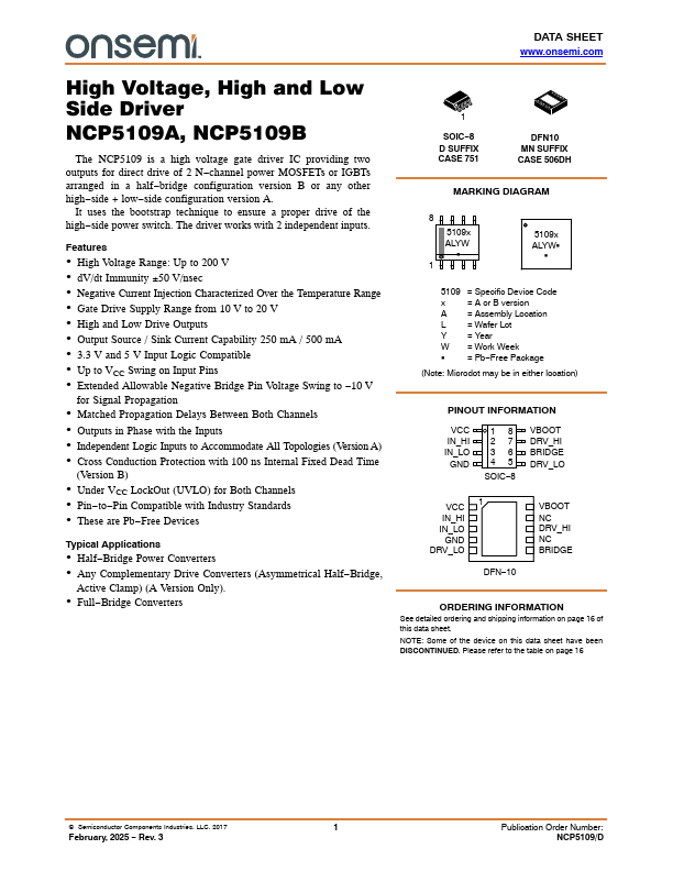
The NCP5109 is a high voltage gate driver IC providing two outputs for direct drive of 2 N−channel power MOSFETs or IGBTs arranged in a half−bridge configuration version B or any other high−side + low−side configuration version A. It uses the bootstrap technique to ensure a proper drive of the high−side power switch. The driver works with 2 independent inputs.| Part No. | NCP5109B |
|---|---|
| Datasheet | NCP5109B Download |
| Manufacturer |  onsemi |
| Description | High and Low Side Driver |
| Buy | Stock & Price |
FEATURES
● High Voltage Range: Up to 200 V● dV/dt Immunity 50 V/nsec
● Negative Current Injection Characterized Over the Temperature Range
● Gate Drive Supply Range from 10 V to 20 V
● High and Low Drive Outputs
● Output Source / Sink Current Capability 250 mA / 500 mA
● 3.3 V and 5 V Input Logic Compatible
● Up to VCC Swing on Input Pins
● Extended Allowable Negative Bridge Pin Voltage Swing to −10 V for Signal Propagation
● Matched Propagation Delays Between Both Channels
● Outputs in Phase with the Inputs
● Independent Logic Inputs to Accommodate All Topologies (Version A)
● Cross Conduction Protection with 100 ns Internal Fixed Dead Time (Version B)
● Under VCC LockOut (UVLO) for Both Channels
● Pin−to−Pin Compatible with Industry Standards
● These are Pb−Free Devices Typical
APPLICATIONS
● Half−Bridge Power Converters● Any Complementary Drive Converters (Asymmetrical Half−Bridge, Active Clamp) (A Version Only).
● Full−Bridge Converters 1 SOIC−8 D SUFFIX CASE 751 DFN10 MN SUFFIX...

