onsemi NCP5201
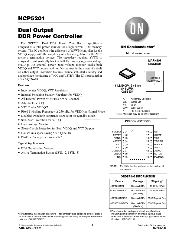
The NCP5201 Dual DDR Power Controller is specifically designed as a total power solution for a high current DDR memory system. This IC combines the efficiency of a PWM controller for the VDDQ supply with the simplicity of a linear regulator for the VTT memory termination voltage. The secondary regulator (VTT) is designed to automatically track at half the primary regulator voltage (VDDQ).| Part No. | NCP5201 |
|---|---|
| Datasheet | NCP5201 Download |
| Manufacturer |  onsemi |
| Description | Dual Output DDR Power Controller |
| Buy | Stock & Price |
FEATURES
MARKING DIAGRAM 1 1 NCP5201 AWLYYWW G G●
●
●
●
●
●
●
●
●
●
●
● Incorporates VDDQ, VTT Regulators Internal Switching Standby Regulator for VDDQ All External Power MOSFETs Are N−Channel Adjustable VDDQ VTT Tracks VDDQ/2 Fixed Switching Frequency of 250 kHz for VDDQ in Normal Mode Doubled Switching Frequency (500 kHz) for Standby Mode Soft−Start Protection for VDDQ Undervoltage Monitor Short−Circuit Protection for Both VDDQ and VTT Outputs Housed in a space saving 5 × 6 QFN−18 Pb−Free Packages are Available* 18−LEAD QFN, 5 x 6 mm MN SUFFIX CASE 505 A = Assembly Location WL = Wafer Lot YY = Year WW = Work Week G = Pb−Free Package (Note: Microdot may be in either location) PIN CONNECTIONS Typical
APPLICATIONS
● DDR Termination Voltage● Active Termination Busses (SSTL−2, SSTL−3) FBDDQ FBVTT PGND VSTBY VTT VTT OCDDQ VDDQ NC 1 2 3 4 5 6 7 8 9 18 17 16 15 14 13 12 11 10 SS COMP VCC TGDDQ BGDDQ SDDQ AGND S3_EN PWRGD NOTE: Pin 19 is the thermal pad on the bottom of the device. ORDERING...

