onsemi NCV3011
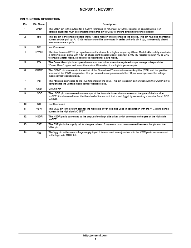
The VREF pin is the output for a 1.25 V reference (1 mA max). This pin has also an internal current source pull up.| Part No. | NCV3011 |
|---|---|
| Datasheet | NCV3011 Download |
| Manufacturer |  onsemi |
| Description | Synchronous PWM Controller |
| Buy | Stock & Price |
FEATURES
● Input Voltage Range from 4.7 V to 28 V● 400 kHz Operation
● 0.8 V $1.0% Reference Voltage
● Buffered External +1.25 V Reference
● Current Limit and Short Circuit Protection
● Power Good
● Enable/Disable Pin
● Input Undervoltage Lockout
● External Synchronization
● Output Overvoltage and Undervoltage Protection
● NCV Prefix for Automotive and Other
APPLICATIONS
Requiring Site and Change Controls● This is a Pb−Free Device Typical
APPLICATIONS
● Set Top Box● Power Modules
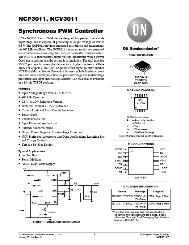
● ASIC / DSP Power Supply VIN CIN EN VCC BST HSDR CBST PG VSW VREF SYNC LSDR R ISET GND Q1 LO Q2 RFB1 RFB2 VOUT CO RREF COMP FB CREF RC CC2 C C1 Figure 1. Typical Application Circuit 14 1 TSSOP−14 DT SUFFIX CASE 948G MARKING DIAGRAM 14 3011 ALYWG G 1 3011= Device Code A = Assembly Location L = Wafer Lot Y = Year W = Work Week G = Pb−Free Package (Note: Microdot may be in either location) VREF EN NC SYNC PG COMP FB PIN CONNECTIONS (TOP VIEW) VCC BST HSDR VSW NC LSDR GND ORDERING INFORMATION Device Package Sh...