onsemi NCV500
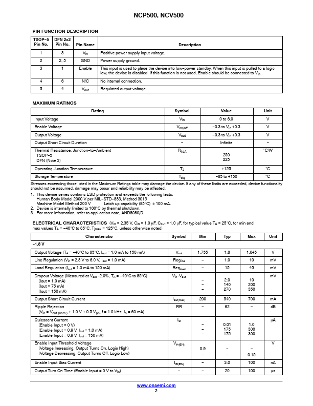
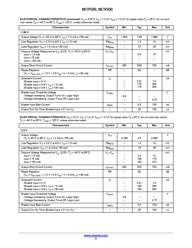
This input is used to place the device into low−power standby. When this input is pulled to a logic low, the device is disabled.| Part No. | NCV500 |
|---|---|
| Datasheet | NCV500 Download |
| Manufacturer |  onsemi |
| Description | 150mA CMOS Low Noise Low-Dropout Voltage Regulator |
| Buy | Stock & Price |
FEATURES
● Ultra−Low Dropout Voltage of 170 mV at 150 mA● Fast Enable Turn−On Time of 20 msec
● Wide Operating Voltage Range of 1.8 V to 6.0 V
● Excellent Line and Load Regulation
● High Accuracy Output Voltage of 2.5%
● Enable Can Be Driven Directly by 1.0 V Logic
● Typical RMS Noise Voltage 50 mV with No Bypass Capacitor (BW = 10 Hz to 100 kHz)
● Very Small DFN 2x2.2 Package
● NCV Prefix for Automotive and Other
APPLICATIONS
Requiring Unique Site and Control Change Requirements; AEC−Q100 Qualified and PPAP Capable● These are Pb−Free Devices Typical
APPLICATIONS
● Noise Sensitive Circuits − VCO’s, RF Stages, etc.● SMPS Post−Regulation
● Hand−Held Instrumentation
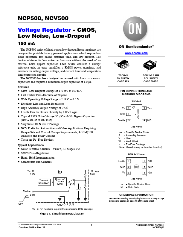
● Camcorders and Cameras Vin 1 (3) Thermal Shutdown Driver w/ Current Limit Vout 5 (4) Enable ON 3 (1) OFF GND 2 (2, 5) NOTE: Pin numbers in parenthesis indicate DFN package. Figure 1. Simplified Block Diagram 5 1 TSOP−5 SN SUFFIX CASE 483 6 1 DFN 2x2.2 MM SQL SUFFIX CASE 506BA PIN CONNECTIONS AND MARKING DIAGRAMS TSOP−5 xx...