onsemi NCV57152
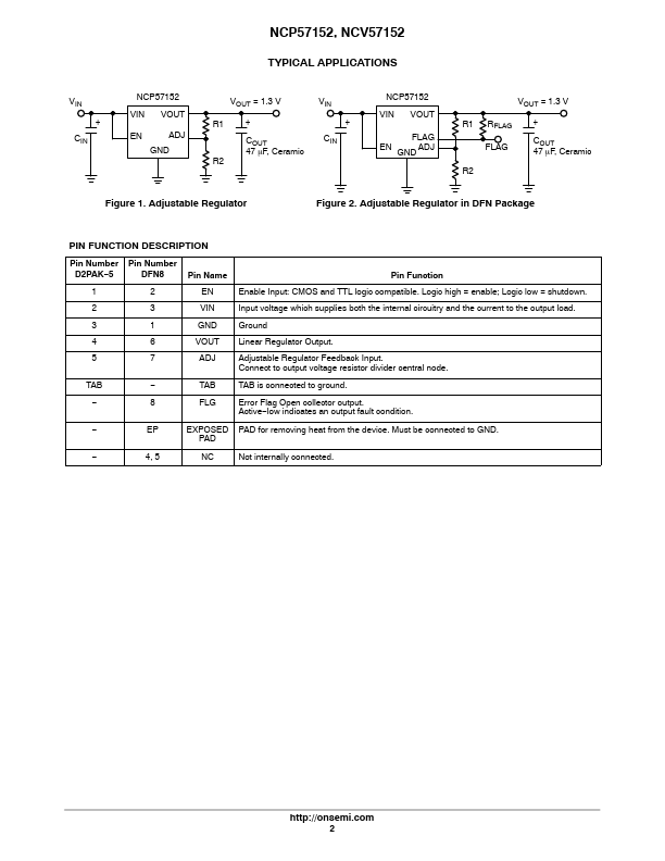
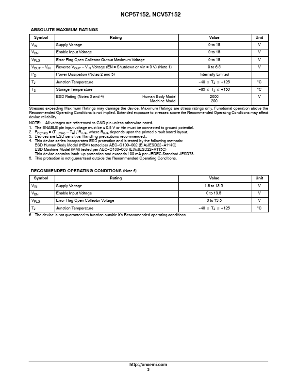
The ENABLE pin input voltage must be 0.8 V or Vin must be connected to ground potential. This device series incorporates ESD protection and is tested by the following methods: ESD Human Body Model (HBM) tested per AEC−Q100−002 (EIA/JESD22−A114C) ESD Machine Model (MM) tested per AEC−Q100−003 (EIA/JESD22−A115C) This device contains latch−up protection and exceeds 100 mA per JEDEC Standard JESD78.- Min Voltage : 1.8V
- Max Voltage : 18V
- Channels : 1
- Max Operating Temp : 125°C
- Min Operating Temp : -40°C
Source:
Octopart
| Part No. | NCV57152 |
|---|---|
| Datasheet | NCV57152 Download |
| Manufacturer |  onsemi |
| Description | 1.5A Very Low-Dropout (VLDO) Fast Transient Response Regulator |
| Buy | Stock & Price |
FEATURES
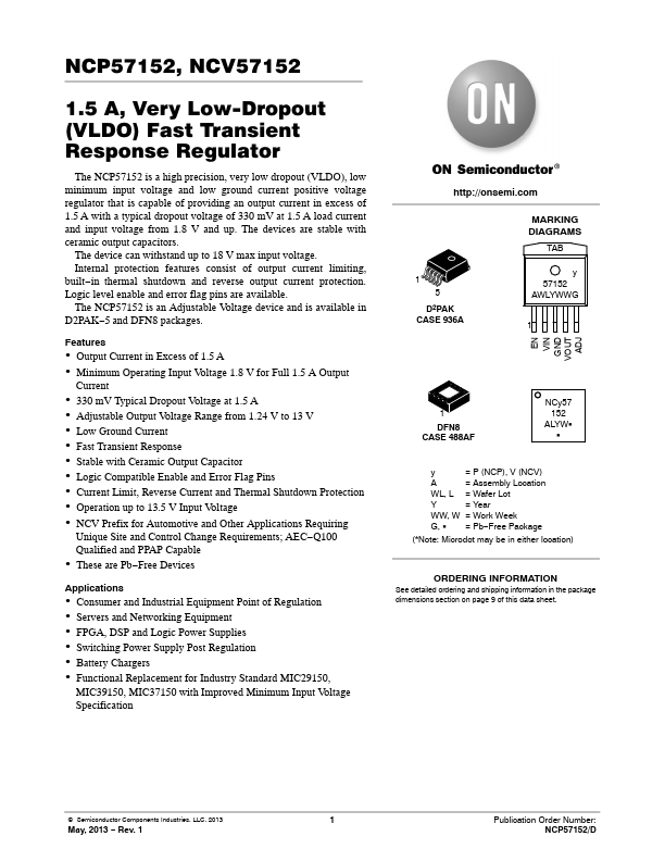
MARKING DIAGRAMS TAB 1 5 D2PAK CASE 936A y 57152 AWLYWWG 1 EN VIN GND VOUT ADJ 1 DFN8 CASE 488AF NCy57 152 ALYWG G y A WL, L Y WW, W G, G = P (NCP), V (NCV) = Assembly Location = Wafer Lot = Year = Work Week = Pb−Free Package (*Note: Microdot may be in either location)● Output Current in Excess of 1.5 A
● Minimum Operating Input Voltage 1.8 V for Full 1.5 A Output
●
●
●
●
●
●
●
●
●
●
●
●
●
●
●
● Current 330 mV Typical Dropout Voltage at 1.5 A Adjustable Output Voltage Range from 1.24 V to 13 V Low Ground Current Fast Transient Response Stable with Ceramic Output Capacitor Logic Compatible Enable and Error Flag Pins Current Limit, Reverse Current and Thermal Shutdown Protection Operation up to 13.5 V Input Voltage NCV Prefix for Automotive and Other
APPLICATIONS
Requiring Unique Site and Control Change Requirements; AEC−Q100 Qualified and PPAP Capable These are Pb−Free Devices Consumer and Industrial Equipment Point of Regulation Servers and Networking Equipment FPGA, DSP and...