onsemi NCV8440
Protected Power MOSFET
| Part No. | NCV8440 |
|---|---|
| Datasheet | NCV8440 Download |
| Manufacturer |  onsemi |
| Description | Protected Power MOSFET |
| Buy | Stock & Price |
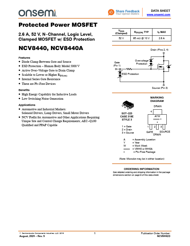
FEATURES
● Diode Clamp Between Gate and Source● ESD Protection − Human Body Model 5000 V
● Active Over−Voltage Gate to Drain Clamp
● Scalable to Lower or Higher RDS(on)
● Internal Series Gate Resistance
● These are Pb−Free Devices Benefits
● High Energy Capability for Inductive Loads
● Low Switching Noise Generation
APPLICATIONS
● Automotive and Industrial Markets: Solenoid Drivers, Lamp Drivers, Small Motor Drivers● NCV Prefix for Automotive and Other
APPLICATIONS
Requiring Unique Site and Control Change Requirements; AEC−Q100 Qualified and PPAP Capable Share Feedback Your Opinion Matters DATA SHEET VDSS (Clamped) 52 V RDS(ON) TYP 95 mW @ 10 V ID MAX 2.6 A Drain (Pins 2, 4) Gate (Pin 1) Overvoltage Protection ESD Protection Source (Pin 3) MARKING DIAGRAM DRAIN SOT−223 CASE 318E STYLE 3 1 = Gate 2 = Drain 3 = Source 4 AYW xxxxx G G 1 23 GATE SOURCE DRAIN A Y W xxxxx G = Assembly Location = Year = Work Week = V8440 or 8440A = Pb−Free Package (Note: Microdot may be in either location)...