onsemi NCV8873
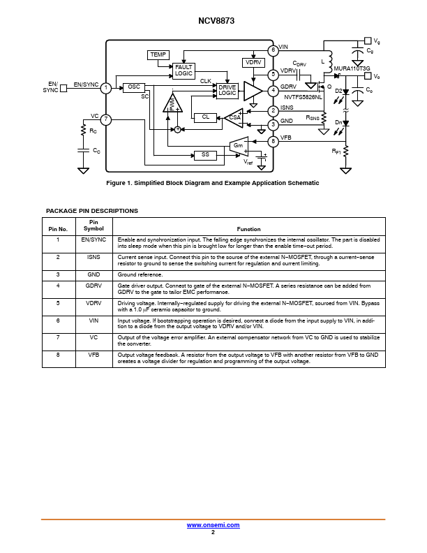
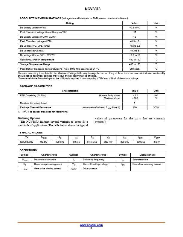
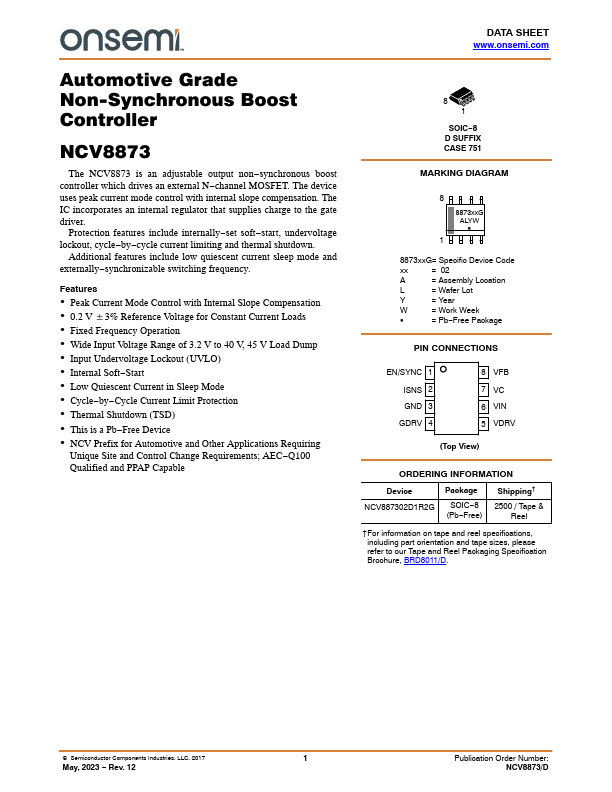
The NCV8873 is an adjustable output non−synchronous boost controller which drives an external N−channel MOSFET. The device uses peak current mode control with internal slope compensation. The IC incorporates an internal regulator that supplies charge to the gate driver.| Part No. | NCV8873 |
|---|---|
| Datasheet | NCV8873 Download |
| Manufacturer |  onsemi |
| Description | Automotive Grade Non-Synchronous Boost Controller |
| Buy | Stock & Price |
FEATURES
● Peak Current Mode Control with Internal Slope Compensation● 0.2 V $3% Reference Voltage for Constant Current Loads
● Fixed Frequency Operation
● Wide Input Voltage Range of 3.2 V to 40 V, 45 V Load Dump
● Input Undervoltage Lockout (UVLO)
● Internal Soft−Start
● Low Quiescent Current in Sleep Mode
● Cycle−by−Cycle Current Limit Protection
● Thermal Shutdown (TSD)
● This is a Pb−Free Device
● NCV Prefix for Automotive and Other
APPLICATIONS
Requiring Unique Site and Control Change Requirements; AEC−Q100 Qualified and PPAP Capable 8 1 SOIC−8 D SUFFIX CASE 751 MARKING DIAGRAM 8 8873xxG ALYW G 1 8873xxG= Specific Device Code xx = 02 A = Assembly Location L = Wafer Lot Y = Year W = Work Week G = Pb−Free Package PIN CONNECTIONS EN/SYNC 1 ISNS 2 GND 3 GDRV 4 8 VFB 7 VC 6 VIN 5 VDRV (Top View) ORDERING INFORMATION Device NCV887302D1R2G Package SOIC−8 (Pb−Free) Shipping† 2500 / Tape & Reel †For information on tape and reel specifications, including part orientation and tape sizes, please refer to our Tape and Reel Packaging Specification Brochure, BRD8011/D. Semiconductor Components Industries, LLC, 2017 1 May, 2023 − Rev.