onsemi NDF03N60Z
N-Channel Power MOSFET
| Part No. | NDF03N60Z |
|---|---|
| Datasheet | NDF03N60Z Download |
| Manufacturer |  onsemi |
| Description | N-Channel Power MOSFET |
| Buy | Stock & Price |
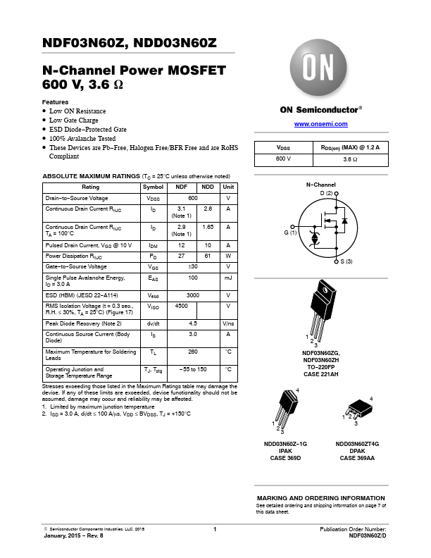
FEATURES
● Low ON Resistance● Low Gate Charge
● ESD Diode−Protected Gate
● 100% Avalanche Tested
● These Devices are Pb−Free, Halogen Free/BFR Free and are RoHS Compliant
ABSOLUTE MAXIMUM RATINGS
(TC = 25°C unless otherwise noted) Rating Symbol NDF NDD Unit Drain−to−Source Voltage Continuous Drain Current RqJC VDSS 600 V ID 3.1 2.6 A (Note 1) Continuous Drain Current RqJC TA = 100°C ID 2.9 1.65 A (Note 1) Pulsed Drain Current, VGS @ 10 V Power Dissipation RqJC Gate−to−Source Voltage Single Pulse Avalanche Energy, ID = 3.0 A ESD (HBM) (JESD 22−A114) RMS Isolation Voltage (t = 0.3 sec., R.H. ≤ 30%, TA = 25°C) (Figure 17) Peak Diode Recovery (Note 2) IDM PD VGS EAS Vesd VISO dv/dt 12 10 A 27 61 W ±30 V 100 mJ 3000 V 4500 V 4.5 V/ns Continuous Source Current (Body IS Diode) 3.0 A Maximum Temperature for Soldering TL Leads 260 °C Operating Junction and Storage Temperature Range TJ, Tstg −55 to 150 °C Stresses exceeding those listed in theMAXIMUM RATINGS
table may damage the device. If any of these limits are exceeded, device functionality should not be assumed, damage may occur and reliability may be affected.