onsemi NDF05N50Z
N-Channel Power MOSFET
| Part No. | NDF05N50Z |
|---|---|
| Datasheet | NDF05N50Z Download |
| Manufacturer |  onsemi |
| Description | N-Channel Power MOSFET |
| Buy | Stock & Price |
FEATURES
●●
●
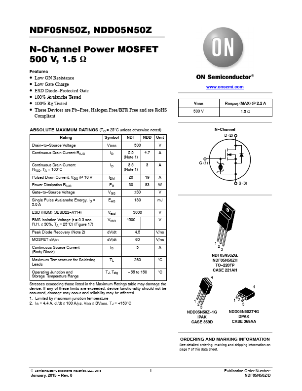
● Low ON Resistance Low Gate Charge 100% Avalanche Tested These Devices are Pb−Free and are RoHS Compliant VDSS 500 V RDS(on) (TYP) @ 2.2 A 1.25 W
ABSOLUTE MAXIMUM RATINGS
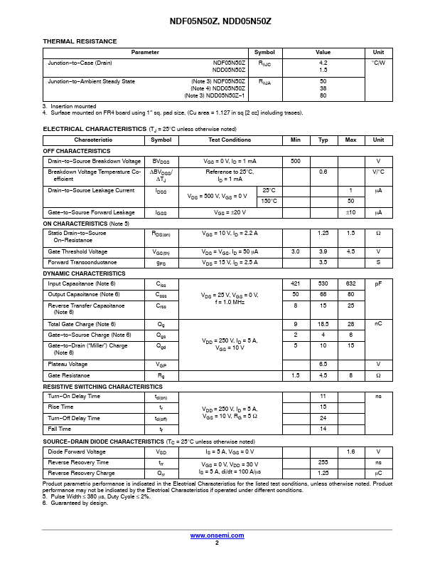
(TC = 25°C unless otherwise noted) Rating Drain−to−Source Voltage Continuous Drain Current RqJC Continuous Drain Current RqJC, TA = 100°C Pulsed Drain Current, VGS @ 10 V Power Dissipation RqJC Gate−to−Source Voltage Single Pulse Avalanche Energy, ID = 5.0 A ESD (HBM) (JESD22−A114) RMS Isolation Voltage (t = 0.3 sec., R.H. ≤ 30%, TA = 25°C) (Figure 15) Peak Diode Recovery Continuous Source Current (Body Diode) Maximum Temperature for Soldering Leads, 0.063″ (1.6 mm) from Case for 10 s Package Body for 10 s Operating Junction and Storage Temperature Range Symbol VDSS ID ID IDM PD VGS EAS Vesd VISO 4500 5 (Note 1) 3.2 (Note 1) 20 (Note 1) 28 NDF NDP 500 5 3.2 20 96 ±30 130 3000 4.7 3 19 83 NDD Unit V A A G (1) A W V mJ V V 4 4 1 2 1 1 3 2 2 3 3 3 DPAK TO−220FP TO−220AB IPAK CASE 221D CASE 221A CASE 369D...