onsemi NIMD6302R2
HDPlus Dual N-Channel Self-protected Field Effect Transistors
| Part No. | NIMD6302R2 |
|---|---|
| Datasheet | NIMD6302R2 Download |
| Manufacturer |  onsemi |
| Description | HDPlus Dual N-Channel Self-protected Field Effect Transistors |
| Buy | Stock & Price |
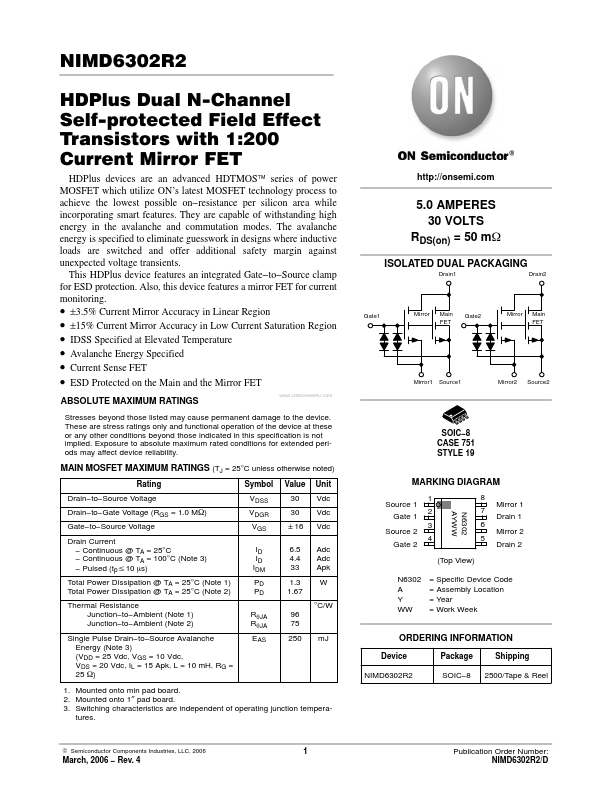
ABSOLUTE MAXIMUM RATINGS
5.0 AMPERES 30 VOLTS RDS(on) = 50 mW ISOLATED DUAL PACKAGING Drain1 Drain2 Gate1 Mirror Main FET Gate2 Mirror Main FET Mirror1 Source1 Mirror2 Source2 Stresses beyond those listed may cause permanent damage to the device. These are stress ratings only and functional operation of the device at these or any other conditions beyond those indicated in this specification is not implied. Exposure to absolute maximum rated conditions for extended periods may affect device reliability. SOIC−8 CASE 751 STYLE 19 MAIN MOSFETMAXIMUM RATINGS
(TJ = 25°C unless otherwise noted) Rating Drain−to−Source Voltage Drain−to−Gate Voltage (RGS = 1.0 MW) Gate−to−Source Voltage Drain Current − Continuous @ TA = 25°C − Continuous @ TA = 100°C (Note 3) − Pulsed (tpv10 ms) Total Power Dissipation @ TA = 25°C (Note 1) Total Power Dissipation @ TA = 25°C (Note 2) Thermal Resistance Junction−to−Ambient (Note 1) Junction−to−Ambient (Note 2) Single Pulse Drain−to−Source Avalanche Energy (Note 3) (VDD = 25 Vdc, VGS = 10 Vdc, VDS = 20 Vdc, IL = 15 Apk, L = 10 mH, RG = 25 W) Symbol VDSS VDGR VGS ID ID IDM PD PD RqJA RqJA EAS Value 30 30 "16 6.