onsemi NIS5112
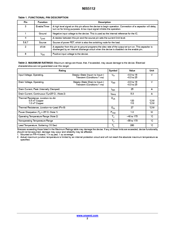
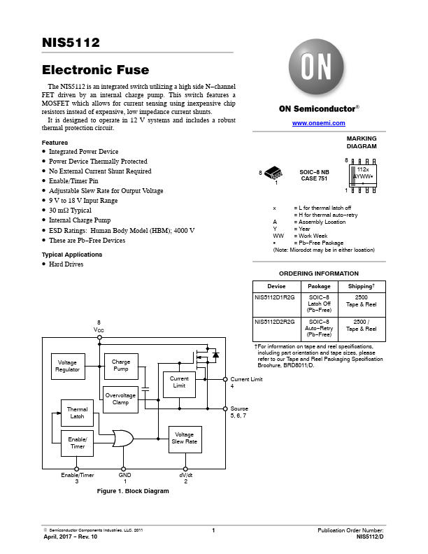
The NIS5112 is an integrated switch utilizing a high side N−channel FET driven by an internal charge pump. This switch features a MOSFET which allows for current sensing using inexpensive chip resistors instead of expensive, low impedance current shunts. It is designed to operate in 12 V systems and includes a robust thermal protection circuit.| Part No. | NIS5112 |
|---|---|
| Datasheet | NIS5112 Download |
| Manufacturer |  onsemi |
| Description | Electronic Fuse |
| Buy | Stock & Price |
FEATURES
● Integrated Power Device● Power Device Thermally Protected
● No External Current Shunt Required
● Enable/Timer Pin
● Adjustable Slew Rate for Output Voltage
● 9 V to 18 V Input Range
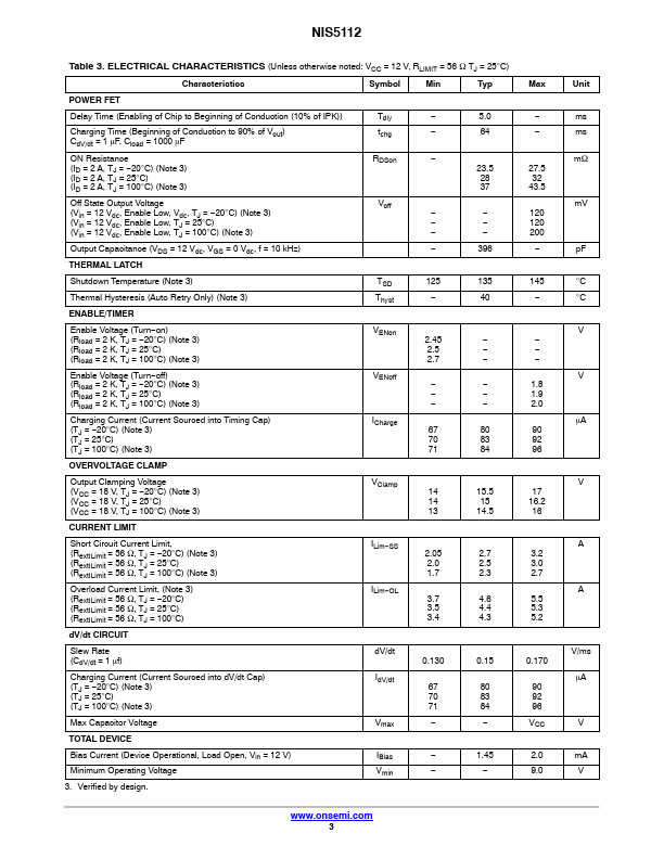
● 30 mW Typical
● Internal Charge Pump
● ESD Ratings: Human Body Model (HBM); 4000 V
● These are Pb−Free Devices Typical
APPLICATIONS
● Hard Drives 8 1 MARKING DIAGRAM SOIC−8 NB CASE 751 8 112x AYWWG G 1 x = L for thermal latch off = H for thermal auto−retry A = Assembly Location Y = Year WW = Work Week G = Pb−Free Package (Note: Microdot may be in either location) ORDERING INFORMATION Device NIS5112D1R2G Package SOIC−8 Latch Off (Pb−Free) Shipping† 2500 Tape & Reel 8 NIS5112D2R2G SOIC−8 2500 / VCC Auto−Retry Tape & Reel (Pb−Free) Voltage Regulator Charge Pump Thermal Latch Overvoltage Clamp Current Limit †For information on tape and reel specifications, including part orientation and tape sizes, please refer to our Tape and Reel Packaging Specification Brochure, BRD8011/D. Current Limit 4 Source 5, 6, 7 Enable/ Timer Voltage Slew Rate Enable/Timer 3 GND 1 Figure 1.