onsemi NL17SV02
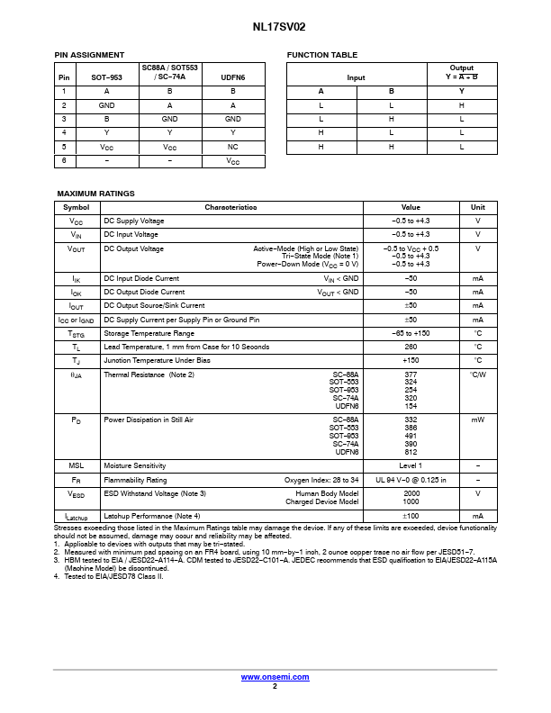
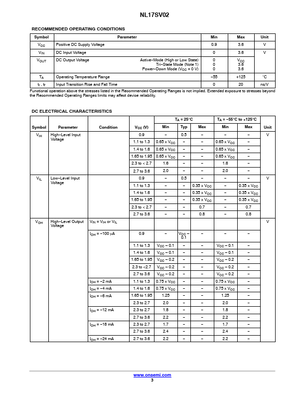
The NL17SV02 is a single 2−input NOR gate in tiny footprint packages. The device is designed to operate for VCC = 0.9 V to 3.6 V.| Part No. | NL17SV02 |
|---|---|
| Datasheet | NL17SV02 Download |
| Manufacturer |  onsemi |
| Description | Single 2-Input NOR Gate |
| Buy | Stock & Price |
FEATURES
● Designed for 0.9 V to 3.6 V VCC Operation● 1.5 ns tPD at 3.3 V (Typ)
● Inputs/Outputs Over−Voltage Tolerant up to 3.6 V
● IOFF Supports Partial Power Down Protection
● Source/Sink 24 mA at 3.3 V
● Available in SOT−353, SOT−553, SOT−953, SC−74A and UDFN 1Packages
● NLV Prefix for Automotive and Other
APPLICATIONS
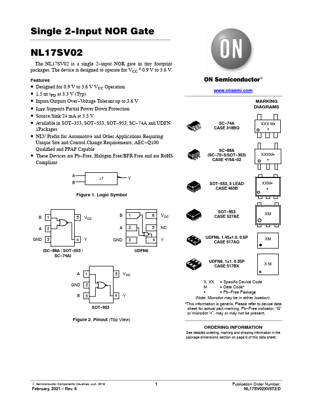
Requiring Unique Site and Control Change Requirements; AEC−Q100 Qualified and PPAP Capable● These Devices are Pb−Free, Halogen Free/BFR Free and are RoHS Compliant A ≥1 Y B Figure 1. Logic Symbol MARKING DIAGRAMS SC−74A CASE 318BQ XXX MG G SC−88A (SC−70−5/SOT−353) CASE 419A−02 XXXMG G SOT−553, 5 LEAD CASE 463B XXMG G B1 A2 5 VCC GND 3 4Y (SC−88A / SOT−553 / SC−74A) B1 A2 6 VCC 5 NC GND 3 4Y UDFN6 A1 GND 2 B3 5 VCC 4Y SOT−953 Figure 2. Pinout (Top View) SOT−953 CASE 527AE XM UDFN6, 1.45x1.0, 0.5P XM CASE 517AQ UDFN6, 1x1, 0.35P CASE 517BX XM X, XX M G = Specific Device Code = Date Code* = Pb−Free Package (Note: Microdot may be in either location) *This information is generic.