onsemi NL7WB66
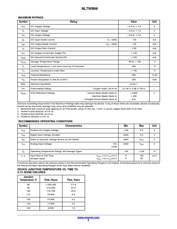
The NL7WB66 is a very low RON dual SPST analog switch. The device is offered in the very popular low cost US8 package. It is designed as a general purpose dual switch and can be used to switch either analog signals such as audio and video or digital signal such as TTL, CMOS, LVDS, ECL, or complex digital signals such as QPSK.| Part No. | NL7WB66 |
|---|---|
| Datasheet | NL7WB66 Download |
| Manufacturer |  onsemi |
| Description | Ultra-Small SPST Analog Switch |
| Buy | Stock & Price |
FEATURES
● Excellent Performance RDSON = 5.0 W at 5.0 V● High Speed Operation: tPD = 0.25 ns (Max) at 5.0 V
● 1.65 to 5.5 V Operating Range
● Reduced Threshold Voltages for LVTTL on Control Pin ♦ Eliminates the Need for Translators for Many
APPLICATIONS
♦ TTL Compatibility when VCC is 5.0 V ♦ Can Operate with 1.8 V Inputs, if VCC is 3.0 ♦ Also Meets Full CMOS Specifications● Ultra−Low Charge Injection = 7.5 pC at 5.0 V
● Low Stand−by Power ICC = 1.0 nA (Max) at TA = 25°C
● Control Pins IN1, IN2, are Overvoltage Tolerant
● Pin for Pin Replacement TC7WB66, NC7WB66, 74LVC2G66
● ESD Protection: Machine Model >200 V, Human Body Model >2000 V
● Latchup Max Rating: 200 mA
● These Devices are Pb−Free, Halogen Free/BFR Free and are RoHS Compliant Typical
APPLICATIONS
● Cell Phones● PDAs
● Digital Still Cameras
● Video
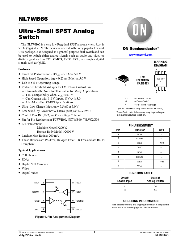
● Digital Video NO1 1 8 VCC COM1 2 7 OE1 OE2 3 6 COM2 GND 4 5 NO2 Figure 1. Pin Assignment Diagram MARKING DIAGRAM 8 8 1 US8 US SUFFIX CASE 493 AJ M G G 1 AJ = Device Code M = Date Code* G = Pb−Free Package (Note: Microdot may be in either location) *Date Code orientation may vary depending upon manufacturing location.