onsemi NLSV1T240
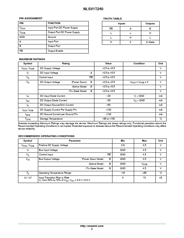
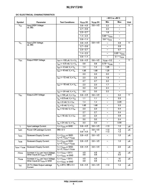
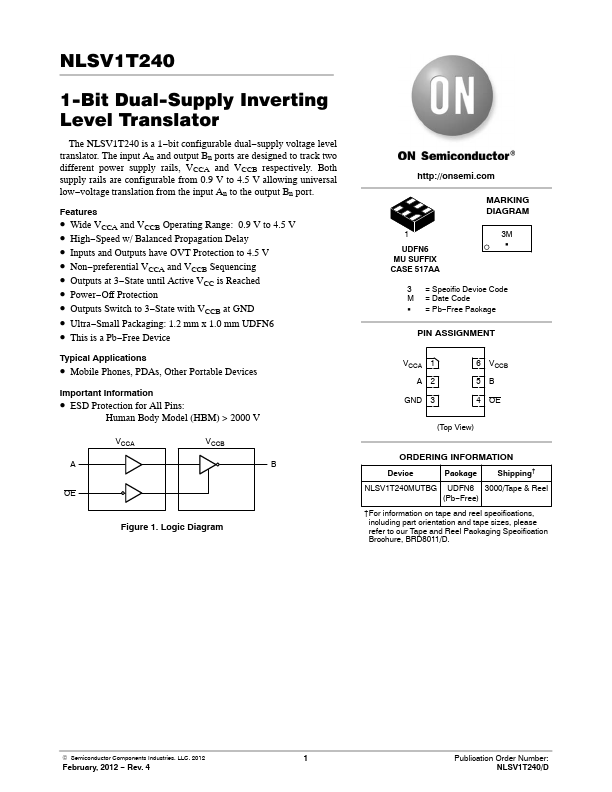
The NLSV1T240 is a 1−bit configurable dual−supply voltage level translator. The input An and output Bn ports are designed to track two different power supply rails, VCCA and VCCB respectively. Both supply rails are configurable from 0.9 V to 4.5 V allowing universal low−voltage translation from the input An to the output Bn port.| Part No. | NLSV1T240 |
|---|---|
| Datasheet | NLSV1T240 Download |
| Manufacturer |  onsemi |
| Description | 1-Bit Dual-Supply Inverting Level Translator |
| Buy | Stock & Price |
FEATURES
● Wide VCCA and VCCB Operating Range: 0.9 V to 4.5 V● High−Speed w/ Balanced Propagation Delay
● Inputs and Outputs have OVT Protection to 4.5 V
● Non−preferential VCCA and VCCB Sequencing
● Outputs at 3−State until Active VCC is Reached
● Power−Off Protection
● Outputs Switch to 3−State with VCCB at GND
● Ultra−Small Packaging: 1.2 mm x 1.0 mm UDFN6
● This is a Pb−Free Device Typical
APPLICATIONS
● Mobile Phones, PDAs, Other Portable Devices Important Information● ESD Protection for All Pins: Human Body Model (HBM) > 2000 V VCCA VCCB AB OE Figure 1. Logic Diagram MARKING DIAGRAM 1 UDFN6 MU SUFFIX CASE 517AA 3M G 3 = Specific Device Code M = Date Code G = Pb−Free Package PIN ASSIGNMENT VCCA 1 A2 GND 3 6 VCCB 5B 4 OE (Top View) ORDERING INFORMATION Device Package Shipping† NLSV1T240MUTBG UDFN6 3000/Tape & Reel (Pb−Free) †For information on tape and reel specifications, including part orientation and tape sizes, please refer to our Tape and Reel Packaging Specification Brochure, BRD8011/D. © Semiconductor Components Industries, LLC, 2012 February, 2012 − Rev.