onsemi NLSV1T34
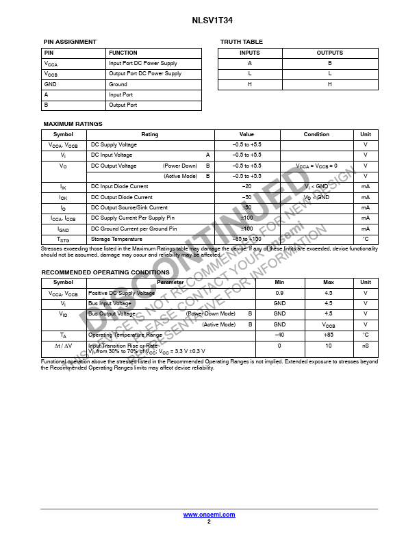
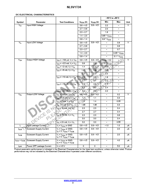
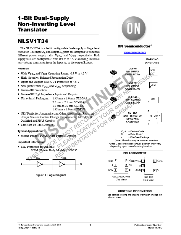
The NLSV1T34 is a 1−bit configurable dual−supply voltage level translator. The input An and output Bn ports are designed to track two different power supply rails, VCCA and VCCB respectively. Both supply rails are configurable from 0.9 V to 4.5 V allowing universal low−voltage translation from the input An to the output Bn port.| Part No. | NLSV1T34 |
|---|---|
| Datasheet | NLSV1T34 Download |
| Manufacturer |  onsemi |
| Description | 1-Bit Dual-Supply Non-Inverting Level Translator |
| Buy | Stock & Price |
FEATURES
● Wide VCCA and VCCB Operating Range: 0.9 V to 4.5 V● High−Speed w/ Balanced Propagation Delay
● Inputs and Outputs have OVT Protection to 4.5 V
● Non−preferential VCCA and VCCB Sequencing
● Power−Off Protection
● Power−Off High Impedance Inputs and Outputs
● Ultra−Small Packaging: 1.45 mm x 1.0 mm ULLGA6 2.0 mm x 2.1 mm SC−88A 1.2 mm x 1.0 mm UDFN6 1.45 mm x 1.0 mm UDFN6
● NLV Prefix for Automotive and Other
APPLICATIONS
Requiring Unique Site and Control Change Requirements; AEC−Q100 Qualified and PPAP Capable● These are Pb−Free Devices Typical
APPLICATIONS
● Mobile Phones, PDAs, Other Portable Devices Important Information● ESD Protection for All Pins: HBM (Human Body Model) > 3000 V VCCA VCCB A B Figure 1. Logic Diagram MARKING DIAGRAMS UDFN6 Q M MU SUFFIX G CASE 517AA 1 UDFN6 MU SUFFIX AM 1 CASE 517AQ ULLGA6 MX1 SUFFIX QM 1 CASE 613AF SC−88A 5 M (SOT−353/SC−70) QMG DF SUFFIX G 1 CASE 419A 1 Q, A = Device Code M = Date Code* G = Pb−Free Package (Note: Microdot may be in either location) *Date Code orientation and/or position may vary depending upon manufacturing location.