onsemi NLSX3014
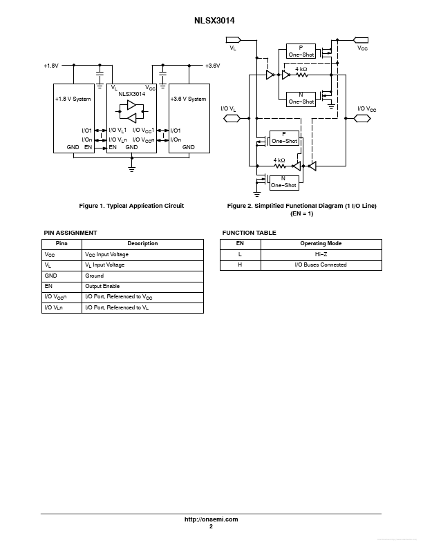
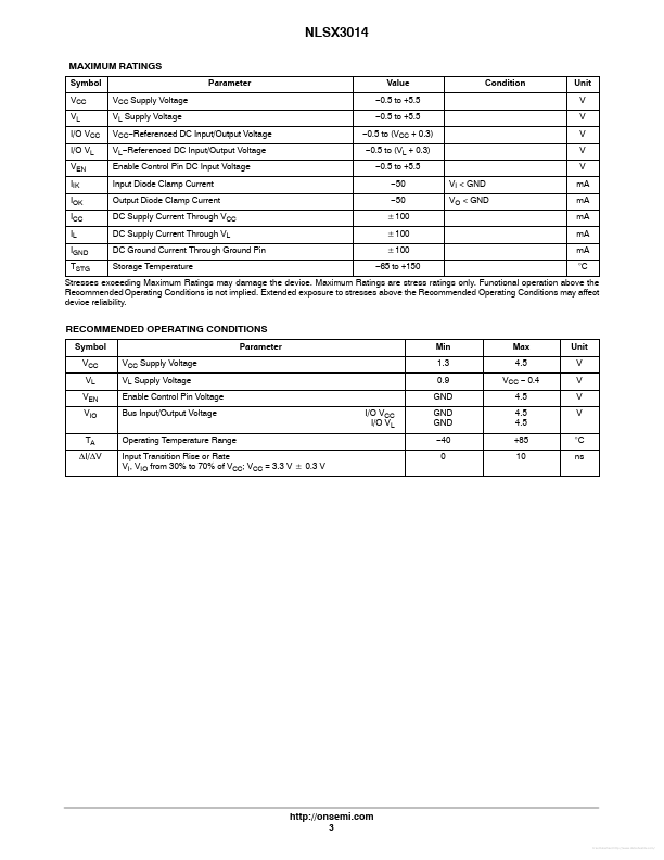
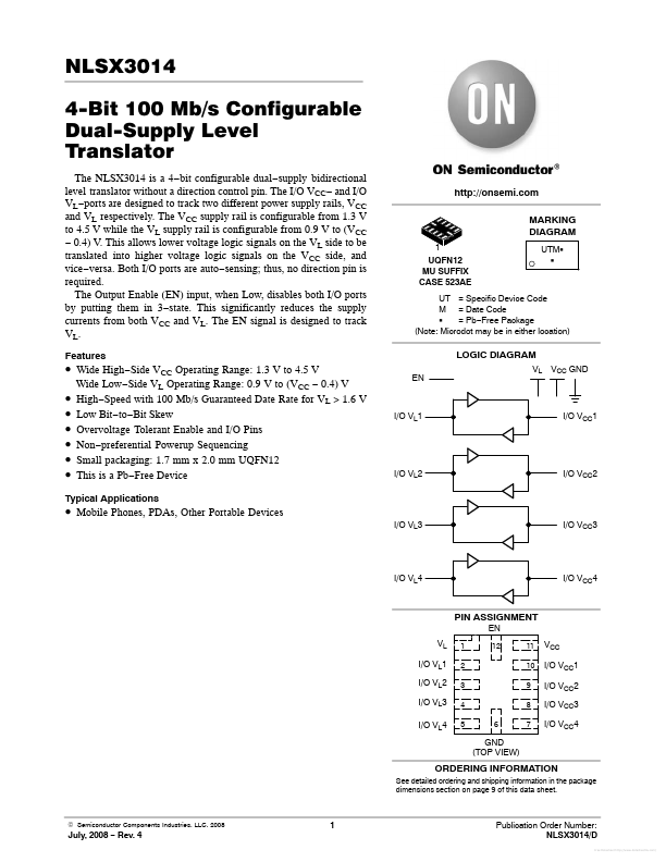
The NLSX3014 is a 4−bit configurable dual−supply bidirectional level translator without a direction control pin. The I/O VCC− and I/O VL−ports are designed to track two different power supply rails, VCC and VL respectively. The VCC supply rail is configurable from 1.3 V to 4.5 V while the VL supply rail is configurable from 0.9 V to (VCC − 0.4) V.| Part No. | NLSX3014 |
|---|---|
| Datasheet | NLSX3014 Download |
| Manufacturer |  onsemi |
| Description | Translator |
| Buy | Stock & Price |
FEATURES
MARKING DIAGRAM 1 UQFN12 MU SUFFIX CASE 523AE UTMG G UT = Specific Device Code M = Date Code G = Pb−Free Package (Note: Microdot may be in either location) LOGIC DIAGRAM EN VL VCC GND● Wide High−Side VCC Operating Range: 1.3 V to 4.5 V
●
●
●
●
●
● Wide Low−Side VL Operating Range: 0.9 V to (VCC − 0.4) V High−Speed with 100 Mb/s Guaranteed Date Rate for VL > 1.6 V Low Bit−to−Bit Skew Overvoltage Tolerant Enable and I/O Pins Non−preferential Powerup Sequencing Small packaging: 1.7 mm x 2.0 mm UQFN12 This is a Pb−Free Device I/O VL1 I/O VCC1 I/O VL2 I/O VCC2 Typical
APPLICATIONS
● Mobile Phones, PDAs, Other Portable Devices I/O VL3 I/O VCC3 I/O VL4 I/O VCC4 PIN ASSIGNMENT EN VL I/O VL1 I/O VL2 I/O VL3 I/O VL4 1 2 3 4 5 6 12 11 10 9 8 7 VCC I/O VCC1 I/O VCC2 I/O VCC3 I/O VCC4 GND (TOP VIEW) ORDERING INFORMATION See detailed ordering and shipping information in the package dimensions section on page 9 of this data sheet. © Semiconductor Components Industries, LLC, 2008 July, 2008 − Rev.