onsemi NSBA144TF3
Digital Transistors
| Part No. | NSBA144TF3 |
|---|---|
| Datasheet | NSBA144TF3 Download |
| Manufacturer |  onsemi |
| Description | Digital Transistors |
| Buy | Stock & Price |
FEATURES
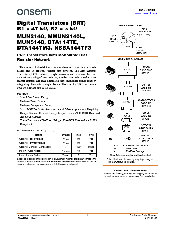
● Simplifies Circuit Design● Reduces Board Space
● Reduces Component Count
● S and NSV Prefix for Automotive and Other
APPLICATIONS
Requiring Unique Site and Control Change Requirements; AEC-Q101 Qualified and PPAP Capable● These Devices are Pb−Free, Halogen Free/BFR Free and are RoHS Compliant
MAXIMUM RATINGS
(TA = 25C) Rating Symbol Max Unit Collector−Base Voltage Collector−Emitter Voltage VCBO 50 Vdc VCEO 50 Vdc Collector Current − Continuous Input Forward Voltage IC 100 VIN(fwd) 40 mAdc Vdc Input Reverse Voltage VIN(rev) 5 Vdc Stresses exceeding those listed in theMAXIMUM RATINGS
table may damage the device. If any of these limits are exceeded, device functionality should not be assumed, damage may occur and reliability may be affected. XX MG G 1 SC−59 CASE 318D STYLE 1 XXX MG G 1 SOT−23 CASE 318 STYLE 6 XX MG G 1 XX M 1 SC−70/SOT−323 CASE 419 STYLE 3 SC−75 CASE 463 STYLE 1 XX M 1 XM 1 SOT−723 CASE 631AA STYLE 1 SOT−1123 CASE 524AA STYLE 1 XXX M G = Specific Device Code = Date Code* = Pb−Free Package (Note: Microdot may be in either location) *Date Code orientation may vary depending upon manufacturing location.