onsemi NSS20101J
20 V 1.0 A / Low VCE(sat) NPN Transistor
| Part No. | NSS20101J |
|---|---|
| Datasheet | NSS20101J Download |
| Manufacturer |  onsemi |
| Description | 20 V 1.0 A / Low VCE(sat) NPN Transistor |
| Buy | Stock & Price |
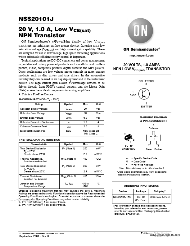
MAXIMUM RATINGS
(TA = 25°C) Rating Collector-Emitter Voltage Collector-Base Voltage Emitter-Base Voltage Collector Current − Continuous Collector Current − Peak Electrostatic Discharge Symbol VCEO VCBO VEBO IC ICM ESD Max 20 40 6.0 1.0 2.0 Unit Vdc Vdc Vdc A A 3 2 20 VOLTS, 1.0 AMPS NPN LOW VCE(sat) TRANSISTOR COLLECTOR 3 1 BASE 2 EMITTER MARKING DIAGRAM & PIN ASSIGNMENT 3 Collector xx M G G 1 Base 2 Emitter HBM Class 3B MM Class C THERMAL CHARACTERISTICS Characteristic Total Device Dissipation TA = 25°C Derate above 25°C Thermal Resistance, Junction−to−Ambient Total Device Dissipation TA = 25°C Derate above 25°C Thermal Resistance, Junction−to−Ambient Junction and Storage Temperature Range Symbol PD (Note 1) Max 255 2.0 RqJA (Note 1) PD (Note 2) 490 300 2.4 RqJA (Note 2) TJ, Tstg 415 −55 to +150 Unit mW mW/°C °C/W mW mW/°C °C/W °C 1 SC−89 CASE 463C xx = Specific Device Code M = Date Code* G = Pb−Free Package (Note: Microdot may be in either location) *Date Code orientation may vary depending upon manufacturing location.