onsemi NTA7002N
Small Signal MOSFET
| Part No. | NTA7002N |
|---|---|
| Datasheet | NTA7002N Download |
| Manufacturer |  onsemi |
| Description | Small Signal MOSFET |
| Buy | Stock & Price |
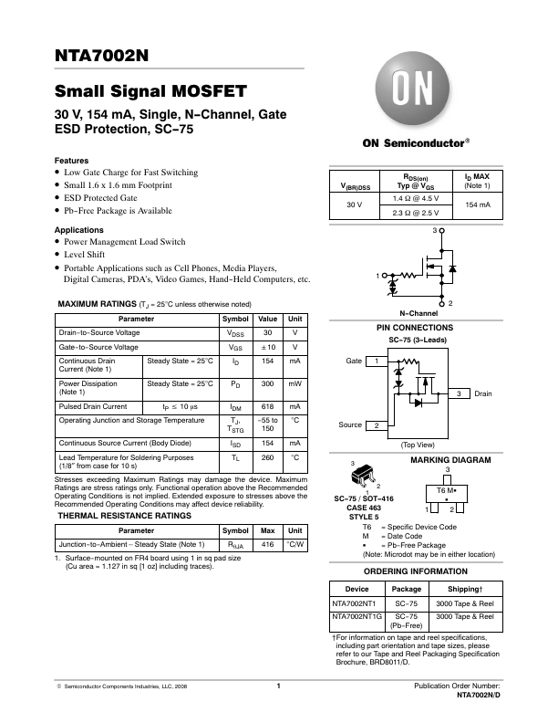
FEATURES
●ăLow Gate Charge for Fast Switching●ăSmall 1.6 x 1.6 mm Footprint
●ăESD Protected Gate
●ăPb-Free Package is Available
APPLICATIONS
●ăPower Management Load Switch●ăLevel Shift
●ăPortable
APPLICATIONS
such as Cell Phones, Media Players, Digital Cameras, PDA's, Video Games, Hand-Held Computers, etc.MAXIMUM RATINGS
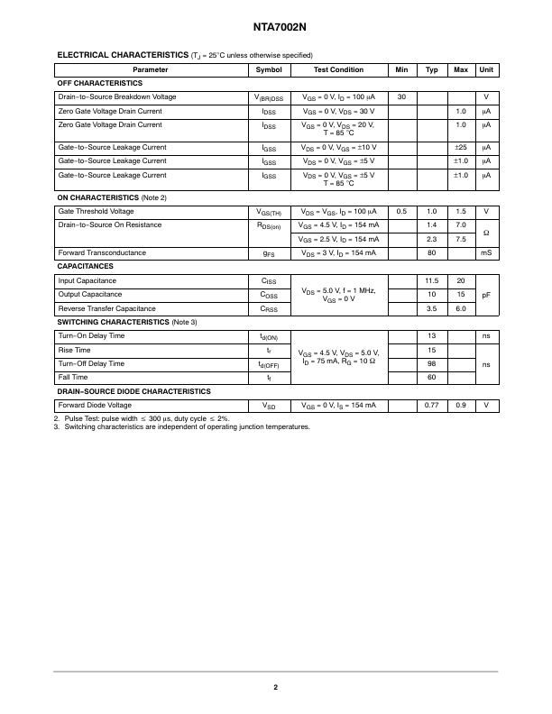
(TJ = 25°C unless otherwise noted) Parameter Symbol Value Unit Drain-to-Source Voltage Gate-to-Source Voltage Continuous Drain Current (Note 1) Steady State = 25°C VDSS VGS ID 30 "10 154 V V mA Power Dissipation (Note 1) Steady State = 25°C PD 300 mW Pulsed Drain Current tP v 10 ms Operating Junction and Storage Temperature Continuous Source Current (Body Diode) Lead Temperature for Soldering Purposes (1/8″ from case for 10 s) IDM TJ, TSTG ISD TL 618 -55 to 150 154 260 mA °C mA °C Stresses exceedingMAXIMUM RATINGS
may damage th