onsemi NTMFS6B03N
Power MOSFET
| Part No. | NTMFS6B03N |
|---|---|
| Datasheet | NTMFS6B03N Download |
| Manufacturer |  onsemi |
| Description | Power MOSFET |
| Buy | Stock & Price |
FEATURES
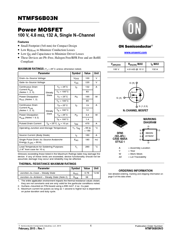
● Small Footprint (5x6 mm) for Compact Design● Low RDS(on) to Minimize Conduction Losses
● Low QG and Capacitance to Minimize Driver Losses
● These Devices are Pb−Free, Halogen Free/BFR Free and are RoHS Compliant
MAXIMUM RATINGS
(TJ = 25°C unless otherwise noted) Parameter Symbol Value Unit Drain−to−Source Voltage Gate−to−Source Voltage Continuous Drain Current RqJC (Notes 1, 2, 3) Power Dissipation RqJC (Notes 1, 2) Steady State TC = 25°C TC = 100°C TC = 25°C TC = 100°C Continuous Drain Current RqJA (Notes 1, 2, 3) Power Dissipation RqJA (Notes 1 & 2) Steady State TA = 25°C TA = 100°C TA = 25°C TA = 100°C Pulsed Drain Current TA = 25°C, tp = 10 ms Operating Junction and Storage Temperature VDSS VGS ID PD ID PD IDM TJ, Tstg 100 ±20 132 83 165 65 19 12 3.4 1.4 470 −55 to + 150 V V A W A W A °C Source Current (Body Diode) Single Pulse Drain−to−Source Avalanche Energy (IL(pk) = 60 A) IS 160 A EAS 180 mJ Lead Temperature for Soldering Purposes (1/8″ from case for 10 s) TL 260 °C Stresses exceeding those listed in theMAXIMUM RATINGS
table may damage the device.