onsemi NTMS4177P
P-Channel Power MOSFET
| Part No. | NTMS4177P |
|---|---|
| Datasheet | NTMS4177P Download |
| Manufacturer |  onsemi |
| Description | P-Channel Power MOSFET |
| Buy | Stock & Price |
FEATURES
● Low RDS(on) to Minimize Conduction Losses● Low Capacitance to Minimize Driver Losses
● Optimized Gate Charge to Minimize Switching Losses
● SOIC−8 Surface Mount Package Saves Board Space
● This is a Pb−Free Device
APPLICATIONS
● Load Switches● Notebook PC’s
● Desktop PC’s
MAXIMUM RATINGS
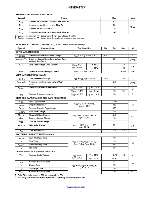
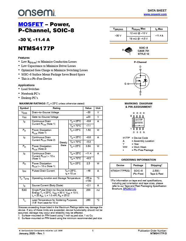
(TJ = 25C unless otherwise stated) Symbol Rating Value Unit VDSS Drain−to−Source Voltage −30 V VGS Gate−to−Source Voltage 20 V ID Continuous Drain Current RqJA (Note 1) TA = 25C −8.9 A TA = 70C −7.1 PD Power Dissipation RqJA (Note 1) TA = 25C 1.52 W ID Continuous Drain TA = 25C −6.6 A Current RqJA (Note 2) Steady TA = 70C −5.3 PD Power Dissipation RqJA (Note 2) State TA = 25C 0.84 W ID Continuous Drain Current RqJA t < 10 s (Note 1) TA = 25C −11.4 A TA = 70C −9.3 PD Power Dissipation RqJA t < 10 s (Note 1) IDM Pulsed Drain Current TA = 25C 2.5 W TA = 25C, tp = 10 ms −46 A TJ, TSTG Operating Junction and Storage Temperature −55 to C +150 IS EAS TL Source Current (Body Diode) Si...