onsemi NTMS4706N
Power MOSFET
| Part No. | NTMS4706N |
|---|---|
| Datasheet | NTMS4706N Download |
| Manufacturer |  onsemi |
| Description | Power MOSFET |
| Buy | Stock & Price |
FEATURES
30 V, 10.3 A, Single N−Channel, SO−8●
●
●
●
●
●
●
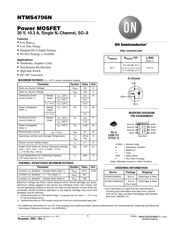
● Low RDS(on) Low Gate Charge Standard SO−8 Single Package Pb−Free Package is Available V(BR)DSS RDS(ON) TYP 9.0 mW @ 10 V 30 V 11.4 mW @ 4.5 V 10.3 A ID MAX (Note 1)
APPLICATIONS
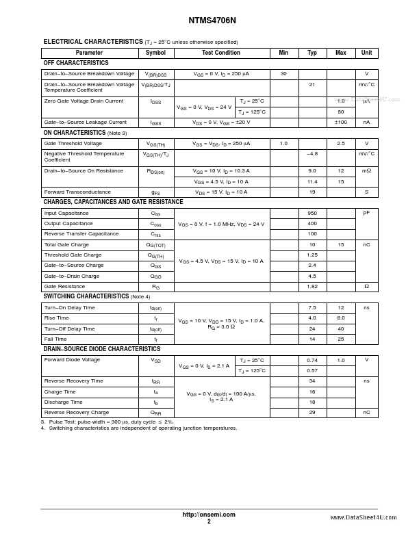
Notebooks, Graphics Cards Synchronous Rectification High Side Switch DC−DC Converters Parameter Symbol VDSS VGS Steady State t v 10 s TA = 25°C TA = 85°C TA = 25°C TA = 25°C PD ID Value 30 ±20 8.6 6.2 10.3 1.5 2.2 TA = 25°C TA = 85°C TA = 25°C tp = 10 ms PD IDM TJ, Tstg IS EAS ID 6.4 4.6 0.83 31 −55 to 150 2.1 150 W A W Unit V V AMAXIMUM RATINGS
(TJ = 25°C unless otherwise stated) Drain−to−Source Voltage Gate−to−Source Voltage Continuous Drain Current (Note 1) N−Channel D G S Power Dissipation (Note 1) Steady State t v 10 s Steady State Continuous Drain Current (Note 2) Power Dissipation (Note 2) Pulsed Drain Current MARKING DIAGRAM/ PIN ASSIGNMENT 1 1 8 Drain Drain Drain Drain 4706N ALYWG G A °C A mJ Operating Junction and Storage Temperature Sourc...