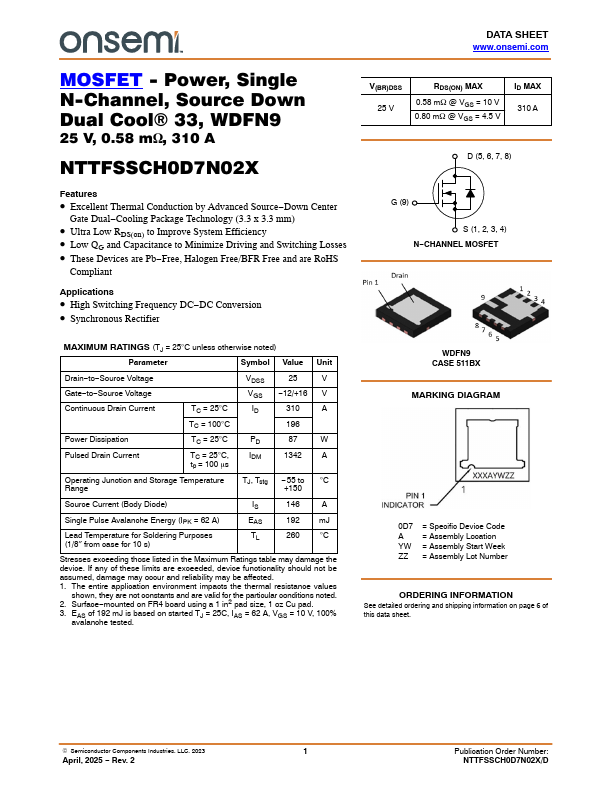
NTTFSSCH0D7N02X
Features
- Excellent Thermal Conduction by Advanced Source- Down Center
Gate Dual- Cooling Package Technology (3.3 x 3.3 mm)
- Ultra Low RDS(on) to Improve System Efficiency
- Low QG and Capacitance to Minimize Driving and Switching Losses
- These Devices are Pb- Free, Halogen Free/BFR Free and are Ro HS pliant
Applications
- High Switching Frequency DC- DC Conversion
- Synchronous Rectifier
V(BR)DSS 25 V
RDS(ON) MAX 0.58 m W @ VGS = 10 V 0.80 m W @ VGS = 4.5 V
ID MAX 310 A
D (5, 6, 7, 8)
G (9)
S (1, 2, 3, 4) N- CHANNEL MOSFET
MAXIMUM RATINGS (TJ = 25°C unless otherwise noted)
Parameter
Symbol Value Unit
Drain- to- Source Voltage
VDSS
Gate- to- Source Voltage
- 12/+16 V
Continuous Drain Current
TC = 25°C
TC = 100°C
Power Dissipation
TC = 25°C
Pulsed Drain Current
TC = 25°C,
IDM tp = 100 ms
1342 A
Operating Junction and Storage Temperature Range
TJ, Tstg
- 55 to °C +150
Source Current (Body...