onsemi NUS5530MN
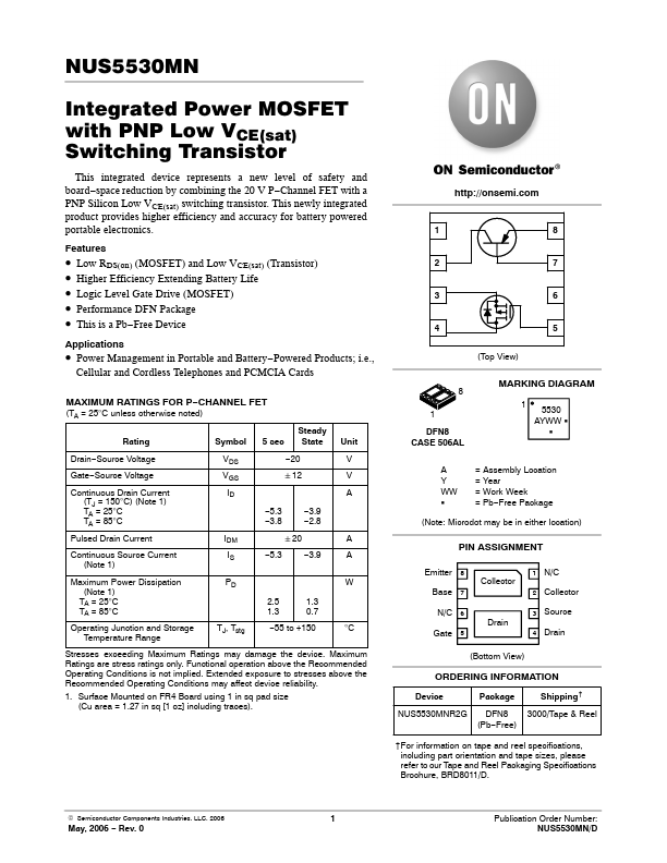
Integrated Power MOSFET
| Part No. | NUS5530MN |
|---|---|
| Datasheet | NUS5530MN Download |
| Manufacturer |  onsemi |
| Description | Integrated Power MOSFET |
| Buy | Stock & Price |
FEATURES
● Low RDS(on) (MOSFET) and Low VCE(sat) (Transistor)● Higher Efficiency Extending Battery Life
● Logic Level Gate Drive (MOSFET)
● Performance DFN Package
● This is a Pb−Free Device
APPLICATIONS
● Power Management in Portable and Battery−Powered Products; i.e., Cellular and Cordless Telephones and PCMCIA CardsMAXIMUM RATINGS
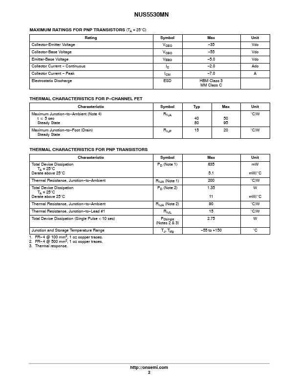
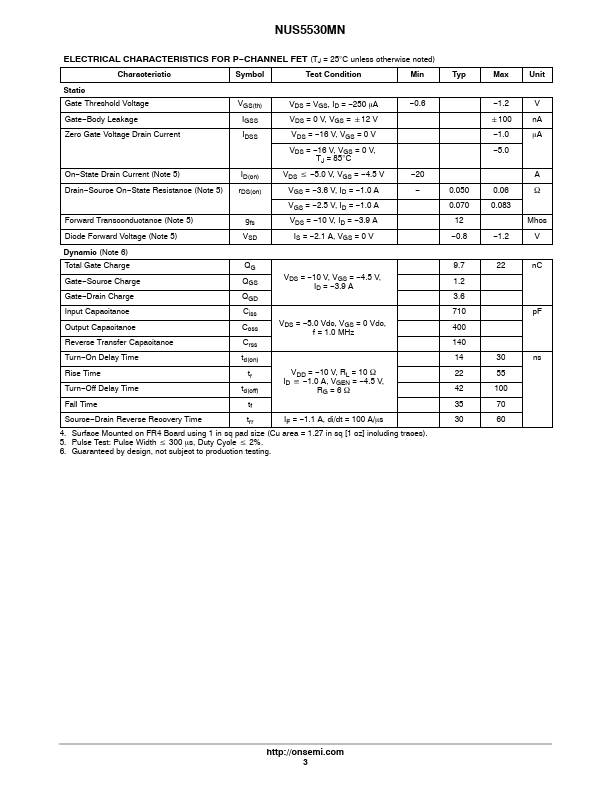
FOR P−CHANNEL FET (TA = 25°C unless otherwise noted) Rating Steady Symbol 5 sec State Unit Drain−Source Voltage Gate−Source Voltage Continuous Drain Current (TJ = 150°C) (Note 1) TA = 25°C TA = 85°C Pulsed Drain Current Continuous Source Current (Note 1) VDS −20 V VGS "12 V ID A −5.3 −3.9 −3.8 −2.8 IDM "20 A IS −5.3 −3.9 A Maximum Power Dissipation (Note 1) TA = 25°C TA = 85°C PD W 2.5 1.3 1.3 0.7 Operating Junction and Storage TJ, Tstg −55 to +150 °C Temperature Range Stresses exceedingMAXIMUM RATINGS
may damage the device.MAXIMUM RATINGS
are stress ratings only. Functional operation above the Recommended Operating Conditions is not implied. Extended exposure to stresses above the Recommended Operating Conditions may affect device reliability.