onsemi NUS6189MN
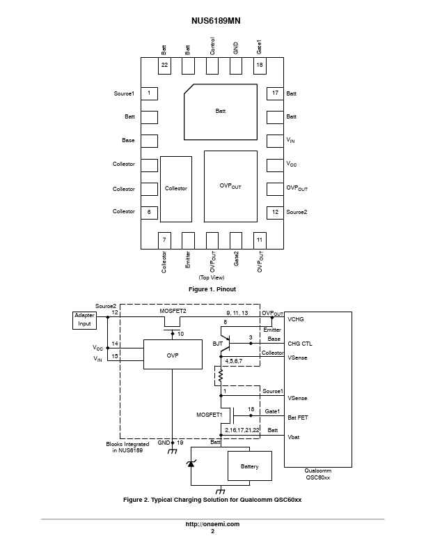
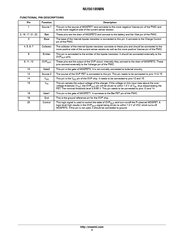
This pin is the source of MOSFET1 and connects to the more negative Vsense pin of the PMIC and to the more negative side of the current sense resistor. It connects to the Charge Control pin of the PMIC.| Part No. | NUS6189MN |
|---|---|
| Datasheet | NUS6189MN Download |
| Manufacturer |  onsemi |
| Description | Low Profile Overvoltage Protection |
| Buy | Stock & Price |
FEATURES
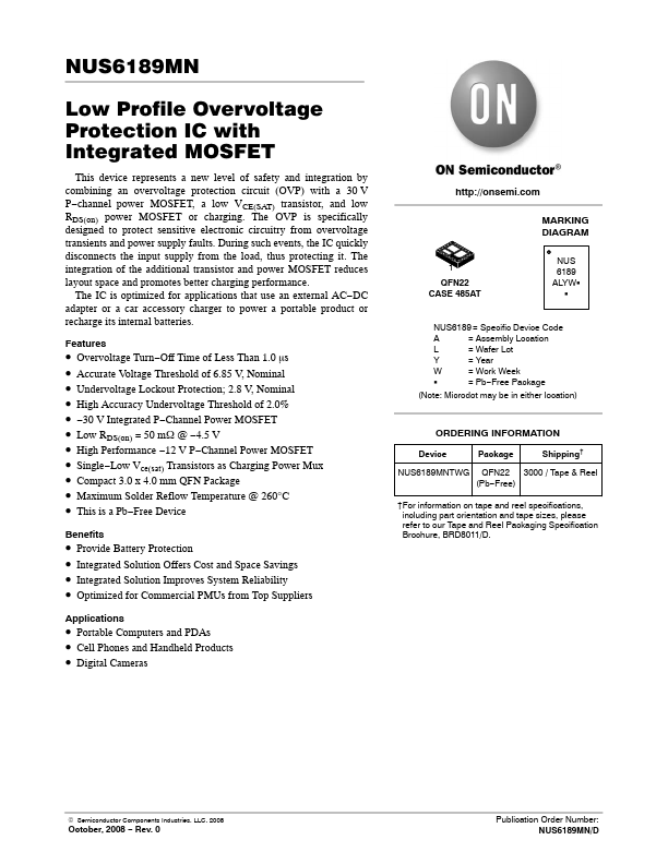
● Overvoltage Turn−Off Time of Less Than 1.0 ms● Accurate Voltage Threshold of 6.85 V, Nominal
● Undervoltage Lockout Protection; 2.8 V, Nominal
● High Accuracy Undervoltage Threshold of 2.0%
● −30 V Integrated P−Channel Power MOSFET
● Low RDS(on) = 50 mW @ −4.5 V
● High Performance −12 V P−Channel Power MOSFET
● Single−Low Vce(sat) Transistors as Charging Power Mux
● Compact 3.0 x 4.0 mm QFN Package
● Maximum Solder Reflow Temperature @ 260°C
● This is a Pb−Free Device Benefits
● Provide Battery Protection
● Integrated Solution Offers Cost and Space Savings
● Integrated Solution Improves System Reliability
● Optimized for Commercial PMUs from Top Suppliers
APPLICATIONS
● Portable Computers and PDAs● Cell Phones and Handheld Products
● Digital Cameras MARKING DIAGRAM 1 QFN22 CASE 485AT NUS 6189 ALYWG G NUS6189 = Specific Device Code A = Assembly Location L = Wafer Lot Y = Year W = Work Week G = Pb−Free Package (Note: Microdot may be in either location) ORDERING INFORMATION D...