onsemi P3P85R01A
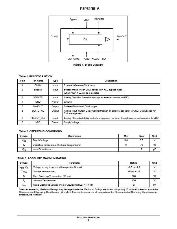
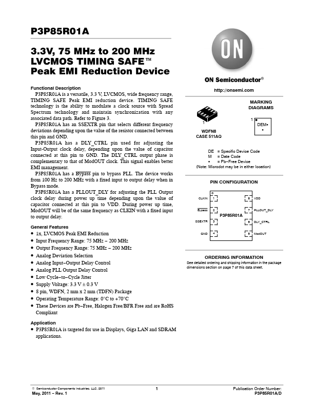
P3P85R01A is a versatile, 3.3 V, LVCMOS, wide frequency range, TIMING SAFE Peak EMI reduction device. P3P85R01A has an SSEXTR pin that selects different frequency deviations depending upon the value of the resistor connected between this pin and GND.| Part No. | P3P85R01A |
|---|---|
| Datasheet | P3P85R01A Download |
| Manufacturer |  onsemi |
| Description | 75 MHz to 200 MHz LVCMOS TIMING SAFE Peak EMI Reduction Device |
| Buy | Stock & Price |
DESCRIPTION
TIMING SAFE technology is the ability to modulate a clock source with Spread Spectrum technology and maintain synchronization with any associated data path. Refer to Figure 3. P3P85R01A has a DLY_CTRL pin used for adjusting the Input-Output clock delay, depending upon the value of capacitor connected at this pin to GND. The DLY_CTRL output phase is complementary to that of ModOUT clock. This signal enables better EMI management. P3P85R01A has a Bypass pin to bypass PLL. The device works from 100 Hz to 200 MHz with a fixed input to output delay when in Bypass mode. P3P85R01A has a PLLOUT_DLY for adjusting the PLL Output clock delay during power up time depending upon the value of capacitor connected at this pin to VDD. During power up time, ModOUT will be of the same frequency as CLKIN with a fixed input to output delay.GENERAL FEATURES
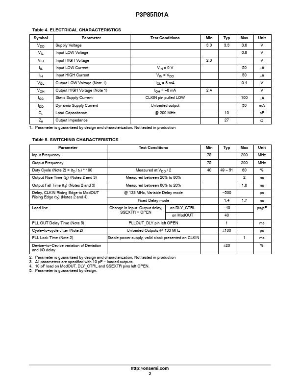
● 1x, LVCMOS Peak EMI Reduction● Input Frequency Range: 75 MHz − 200 MHz
● Output Frequency Range: 75 MHz − 200 MHz
● Analog Deviation Sel...