PCFF75H120SWF
Features
- Advanced Gen VII Technology
- Fast and Soft Recovery
- Maximum Junction Temperature 175°C
- Low Forward Voltage: VF = 1.78 V (Typ.) @ IF = 75 A
- Easy to Parallel Operation
Typical Applications
- Solar
- Energy Storage
- Industrial Motor Control
MECHANICAL PARAMETERS
Parameter Die Size (w/ Scribe Lane) Anode Pad Size Scribe Lane Width Die Thickness Top Metal
Value
Unit
3,900 x 7,000 mm2
2,917 x 6,017 mm2
80 mm
119 mm
6 mm Al Si Cu
Back Metal Topside Passivation Wafer Diameter
1.65 mm Ti/Ni V/Ag Silicon Nitride plus Polyimide
200 mm
Max Possible Die Per
Wafer
Remended Storage Environment
In original container, in dry nitrogen, < 6 months at an ambient temperature of 23°C
DIE DATA SHEET .onsemi.
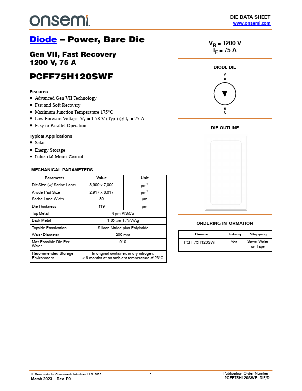
VR = 1200 V IF = 75 A
DIODE DIE A
C DIE OUTLINE
ORDERING INFORMATION
Device PCFF75H120SWF
Inking Yes
Shipping
Sawn Wafer on Tape
© Semiconductor ponents Industries, LLC, 2015
March 2023
- Rev....