onsemi PCS1P2192A
The PCS1P2192A is a clock generator that generates multiple selectable pixel clock outputs for Video Display Panel applications from an external 20MHz reference clock. The PLL based clock generator is specifically designed to provide zero ppm frequency synthesis error on all clock outputs. The device is available in an 8-pin SOIC package.| Part No. | PCS1P2192A |
|---|---|
| Datasheet | PCS1P2192A Download |
| Manufacturer |  onsemi |
| Description | VDP Multiple Pixel Clock Generator |
| Buy | Stock & Price |
FEATURES
● Generates multiple clock outputs from 20MHz external reference clock● Input frequency: 20MHz
● Output frequencies: o Selectable CLKOUT: 108MHz, 27MHz, 33.2MHz, 85MHz, 65MHz, 25MHz, 45MHz, and 40MHz o REFOUT: 20MHz
● Operating Supply Voltage: 3.3V ± 0.3V
● Zero ppm frequency synthesis error on all clock outputs
● 8-pin SOIC package Product
DESCRIPTION
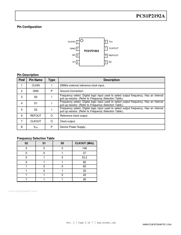
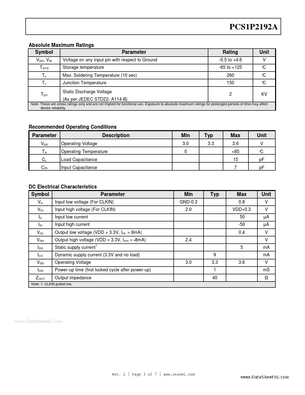
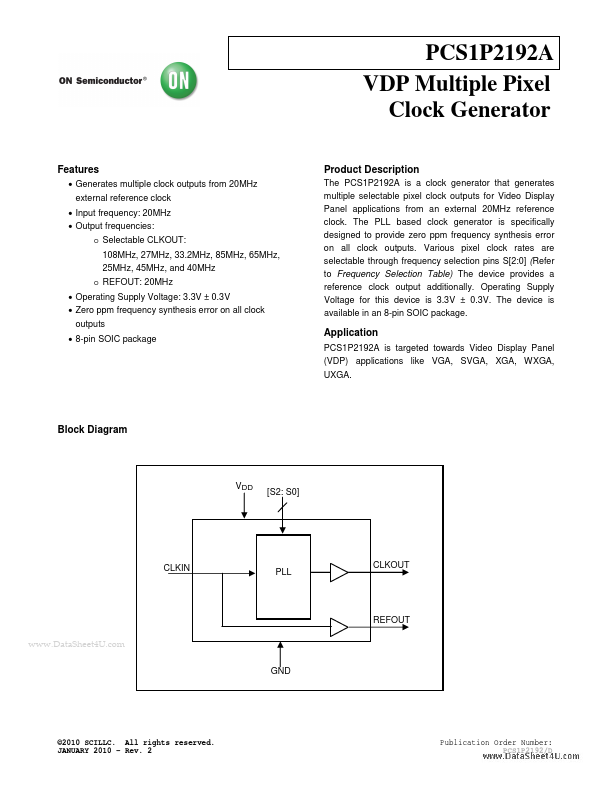
Various pixel clock rates are selectable through frequency selection pins S[2:0] (Refer to Frequency Selection Table) The device provides a reference clock output additionally. Operating Supply Voltage for this device is 3.3V ± 0.3V. The device is available in an 8-pin SOIC package. Application PCS1P2192A is targeted towards Video Display Panel (VDP) applications like VGA, SVGA, XGA, WXGA, UXGA. Block Diagram VDD [S2: S0] CLKIN PLL CLKOUT REFOUT GND ©2010 SCILLC. All rights reserved. JANUARY 2010 – Rev. 2 Publication Order Number: PCS1P2192/D PCS1P2192A Pin Configuration CLKIN 1 GND 2 PCS1P2192A S0 3 S1 4 8 7 VDD CLKOUT REFOUT...