onsemi PCS3P623Z09B
PCS3P623Z05/09 is a versatile, 3.3 V Zero−delay buffer designed to distribute Timing−Safe clocks with Peak EMI reduction.| Part No. | PCS3P623Z09B |
|---|---|
| Datasheet | PCS3P623Z09B Download |
| Manufacturer |  onsemi |
| Description | Peak EMI Reduction IC |
| Buy | Stock & Price |
DESCRIPTION
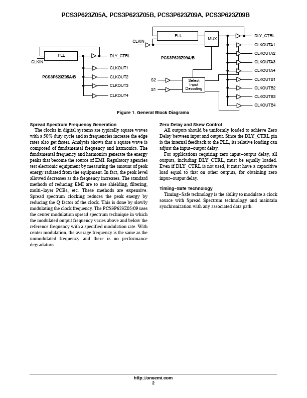
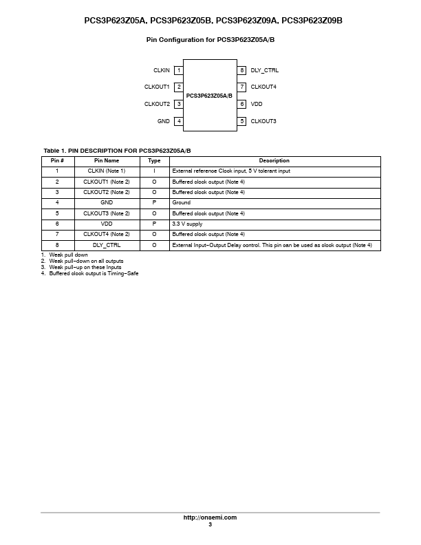
PCS3P623Z05 is an eight−pin version, accepts one reference input and drives out five low−skew Timing−Safe clocks. PCS3P623Z09 accepts one reference input and drives out nine low−skew Timing−Safe clocks. PCS3P623Z05/09 has a DLY_CTRL for adjusting the Input−Output clock delay, depending upon the value of capacitor connected at this pin to GND. PCS3P623Z05/09 operates from a 3.3 V supply and is available in two different packages, as shown in the ordering information table, over commercial and Industrial temperature range. Application PCS3P623Z05/09 is targeted for use in Displays and memory interface systems.FEATURES
● Clock Distribution with Timing−Safe Peak EMI Reduction● Input Frequency Range: 20 MHz − 50 MHz
● Multiple Low Skew Timing−Safe Outputs: PCS3P623Z05: 5 Outputs PCS3P623Z09: 9 Outputs
● External Input−Output Delay Control Option
● Supply Voltage: 3.3 V ± 0.3 V
● Commercial and Industrial Temperature Range
● Packaging Information: ASM3P623Z05: 8 pin SOIC, and T...