onsemi SN74LS299
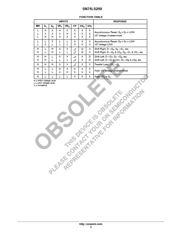
The SN74LS299 is an 8-Bit Universal Shift/Storage Register with 3-state outputs. The parallel load inputs and flip-flop outputs are multiplexed to reduce the total number of package pins.| Part No. | SN74LS299 |
|---|---|
| Datasheet | SN74LS299 Download |
| Manufacturer |  onsemi |
| Description | 8-Bit Shift/Storage Register |
| Buy | Stock & Price |
APPLICATIONS
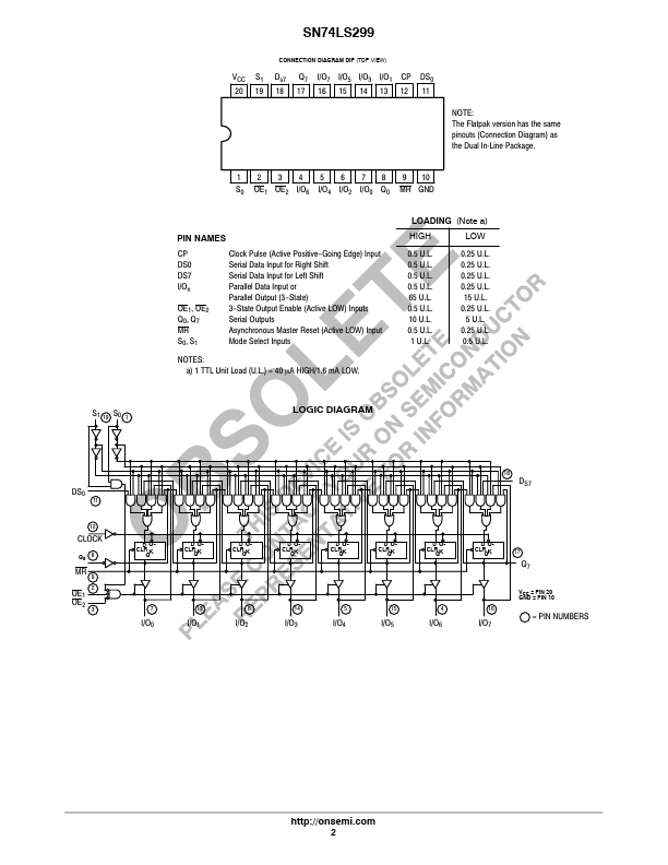
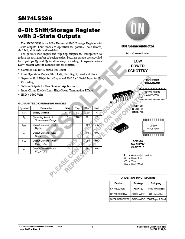
● Input Clamp Diodes Limit High-Speed Termination Effects● ESD > 3500 Volts LOW POWER SCHOTTKY MARKING DIAGRAMS SN74LS299N AWLYYWW GUARANTEED OPERATING RANGES Symbol Parameter Min Typ Max Unit VCC Supply Voltage TA Operating Ambient Temperature Range 4.75 5.0 5.25 V 0 25 70 °C IOH Output Current − High Q0, Q7 IOL Output Current − Low Q0, Q7 IOH Output Current − High I/O0 − 1/O7 IOL Output Current − Low I/O0 − 1/O7 −0.4 mA 8.0 mA −2.6 mA 24 mA 20 1 1 PDIP−20 N SUFFIX CASE 738 20 1 LS299 AWLYYWW 1 SOIC−20 DW SUFFIX CASE 751D A = Assembly Location WL = Wafer Lot YY = Year WW = Work Week ORDERING INFORMATION Device Package Shipping SN74LS299N PDIP−20 1440 Units/Box SN74LS299DW SOIC−WIDE 38 Units/Rail SN74LS299DWR2 SOIC−WIDE 2500/Tape & Reel © Semiconductor Components Industries, LLC, 2006 1 July, 2006 − Rev. 9 Publication Order Number: SN74LS299/D S1 19 S0 1 SN74LS299 CONNECTION DIAGRAM DIP (TOP VIEW) VCC S1 Ds7 Q7 I/O7 I/O5 I/O3 I/O1 CP DS0 20 19 18 17 16 15 14 13 12 11 NOTE: The Flatpak version has the same pinouts (Connection Diagram) as the Dual In-Line Package.