onsemi SZESD7451
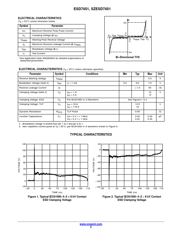
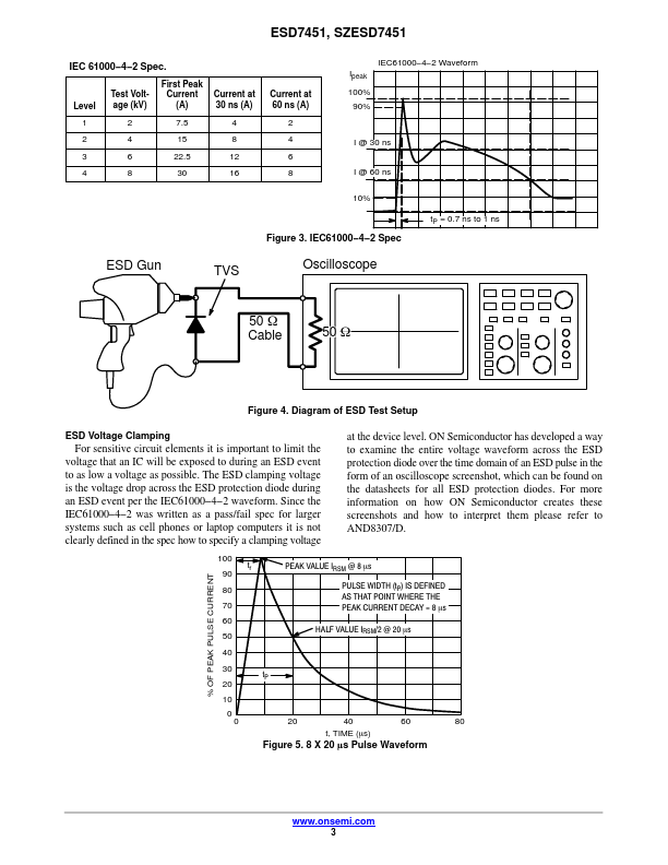
The ESD clamping voltage is the voltage drop across the ESD protection diode during an ESD event per the IEC61000−4−2 waveform.| Part No. | SZESD7451 |
|---|---|
| Datasheet | SZESD7451 Download |
| Manufacturer |  onsemi |
| Description | ESD Protection Diode |
| Buy | Stock & Price |
FEATURES
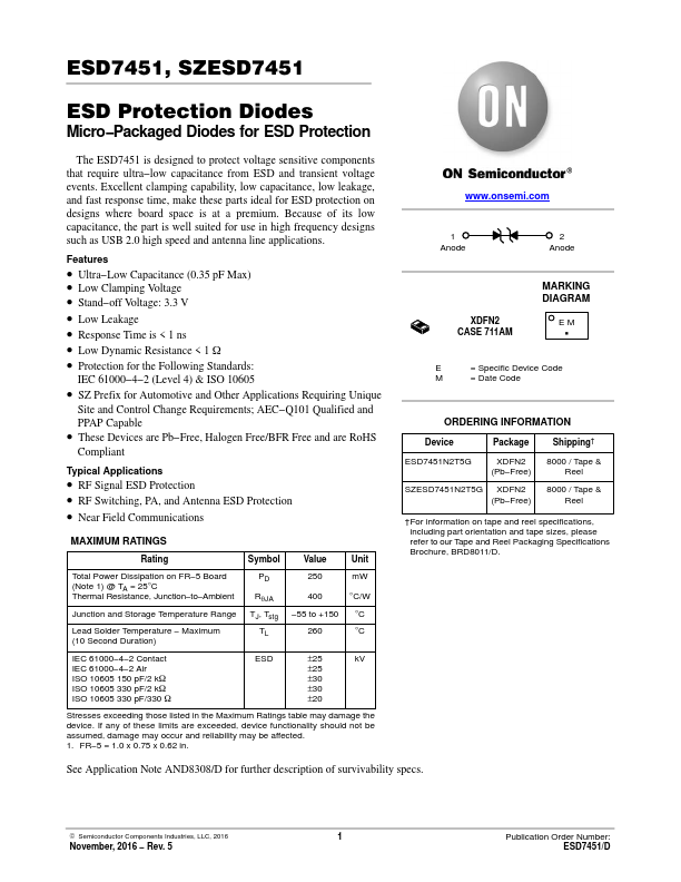
● Ultra−Low Capacitance (0.35 pF Max)● Low Clamping Voltage
● Stand−off Voltage: 3.3 V
● Low Leakage
● Response Time is < 1 ns
● Low Dynamic Resistance < 1 W
● Protection for the Following Standards: IEC 61000−4−2 (Level 4) & ISO 10605
● SZ Prefix for Automotive and Other
APPLICATIONS
Requiring Unique Site and Control Change Requirements; AEC−Q101 Qualified and PPAP Capable● These Devices are Pb−Free, Halogen Free/BFR Free and are RoHS Compliant Typical
APPLICATIONS
● RF Signal ESD Protection● RF Switching, PA, and Antenna ESD Protection
● Near Field Communications
MAXIMUM RATINGS
Rating Symbol Value Unit Total Power Dissipation on FR−5 Board (Note 1) @ TA = 25°C Thermal Resistance, Junction−to−Ambient Junction and Storage Temperature Range Lead Solder Temperature − Maximum (10 Second Duration) °PD° RqJA TJ, Tstg TL 250 mW 400 °C/W −55 to +150 °C 260 °C IEC 61000−4−2 Contact IEC 61000−4−2 Air ISO 10605 150 pF/2 kW ISO 10605 330 pF/2 kW ISO 10605 330 pF/330 W ESD ±25 kV ±25 ±30 ±30 ±20 Stresses exceeding those listed in theMAXIMUM RATINGS
table may damage the device.