onsemi T40N03G
Power MOSFET
| Part No. | T40N03G |
|---|---|
| Datasheet | T40N03G Download |
| Manufacturer |  onsemi |
| Description | Power MOSFET |
| Buy | Stock & Price |
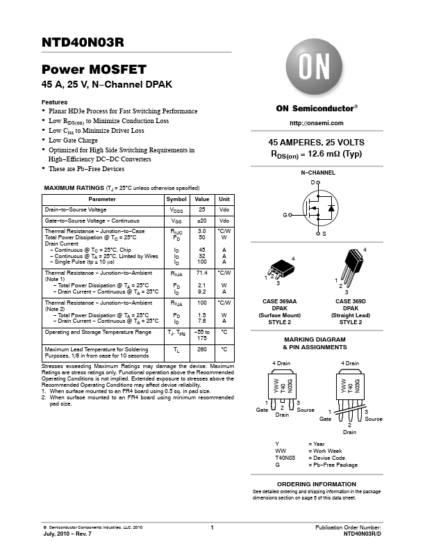
FEATURES
● Planar HD3e Process for Fast Switching Performance● Low RDS(on) to Minimize Conduction Loss
● Low Ciss to Minimize Driver Loss
● Low Gate Charge
● Optimized for High Side Switching Requirements in High−Efficiency DC−DC Converters
● These are Pb−Free Devices
MAXIMUM RATINGS
(TJ = 25°C unless otherwise specified) Parameter Symbol Value Unit Drain−to−Source Voltage Gate−to−Source Voltage − Continuous Thermal Resistance − Junction−to−Case Total Power Dissipation @ TC = 25°C Drain Current − Continuous @ TC = 25°C, Chip − Continuous @ TA = 25°C, Limited by Wires − Single Pulse (tp ≤ 10 ms) Thermal Resistance − Junction−to−Ambient (Note 1) − Total Power Dissipation @ TA = 25°C − Drain Current − Continuous @ TA = 25°C Thermal Resistance − Junction−to−Ambient (Note 2) − Total Power Dissipation @ TA = 25°C − Drain Current − Continuous @ TA = 25°C Operating and Storage Temperature Range VDSS VGS RPqDJC ID ID ID RqJA PD ID RqJA PD ID TJ, Tstg 25 ±20 3.0 50 45 32 100 71.4 2.1 9.2 100 1.
