onsemi TF252
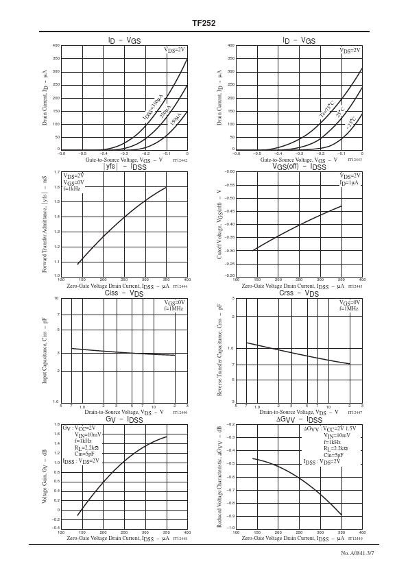
The TF252 is classified by IDSS as follows : (unit : μA) Rank 4 5 IDSS 140 to 240 210 to 350 Test Circuit Voltage gain Frequency Characteristic Distortion Reduced Voltage Characteristic 2.2kΩ 5pF 33μF + VCC=2V VCC=1.5V OSC VTVM V THD min --20 --0.1 140* 0.8 Ratings typ --0.4 1.4 3.1 0.95 max --1.0 350* Unit V V μA mS pF pF 1.0 --0.6 0.65 --106 --2.0 --1.0 --102 dB dB dB % dB Ordering Information Device TF252-4-TL-H TF252-5-TL-H Package USFP USFP Shipping 10,000pcs./reel 10,000pcs./reel memo Pb Free and Halogen Free Drain Current, ID -- μA Drain Current, ID -- μA ID -- VDS 300 250 VGS=0V 200...| Part No. | TF252 |
|---|---|
| Datasheet | TF252 Download |
| Manufacturer |  onsemi |
| Description | N-Channel JFET |
| Buy | Stock & Price |

FEATURES
● High gain : GV=1.0dB typ (VCC=2V, RL=2.2kΩ, Cin=5pF, VIN=10mV, f=1kHz)● Ultrasmall package facilitates miniaturization in end products [1.0mm×0.6mm×0.27mm (max 0.3mm)]
● Best suited for use in Electret Condenser Microphone for audio equipments and telephones
● Excellent voltage characteristics
● Excellent transient characteristics
● Adoption of FBET process
● Halogen free compliance
● Protection diode in Specifications
ABSOLUTE MAXIMUM RATINGS
at Ta=25°C Parameter Symbol Gate-to-Drain Voltage Gate Current Drain Current Allowable Power Dissipation Junction Temperature VGDO IG ID PD Tj Storage Temperature Tstg Conditions Ratings --20 10 1 30 150 --55 to +150 Unit V mA mA mW °C °C Stresses exceedingMAXIMUM RATINGS
may damage the device.MAXIMUM RATINGS
are stress ratings only. Functional operation above the Recommended Operating Conditions is not implied. Extended exposure to stresses above the Recommended Operating Conditions may affect device reliability. LOT No. LOT No. Pac...