onsemi TF412S
N-Channel JFET
| Part No. | TF412S |
|---|---|
| Datasheet | TF412S Download |
| Manufacturer |  onsemi |
| Description | N-Channel JFET |
| Buy | Stock & Price |

FEATURES
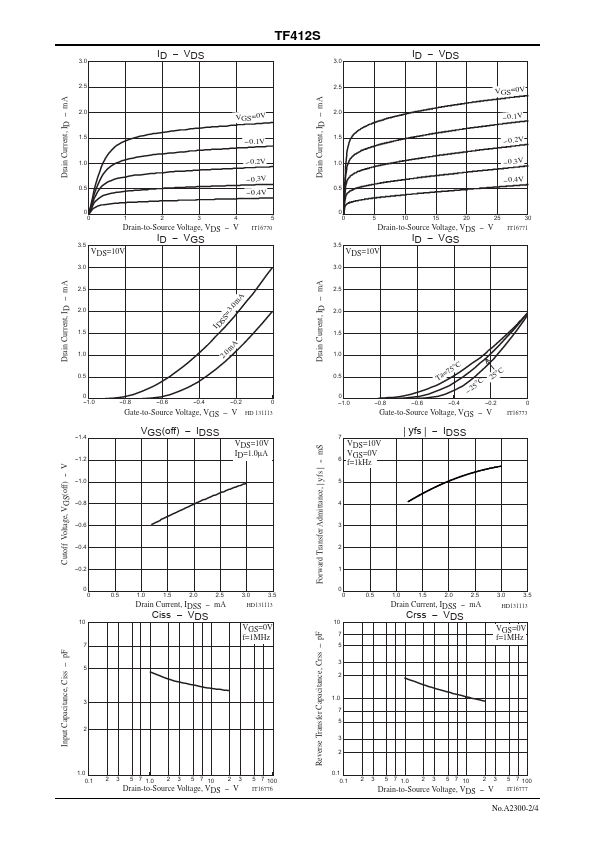
● Small IGSS : max 1.0nA (VGS= 20V, VDS=0V)● Small Ciss : typ 4pF (VDS=10V, VGS=0V, f=1MHz)
● Ultrasmall package facilitates miniaturization in end products
● Halogen free compliance
APPLICATIONS
● Low-Frequency general-purpose amplifier, impedance conversion, infrared sensor applications Electrical Connection 3 1 : Source 2 : Drain 3 : Gate 1 2 Top view SpecificationsABSOLUTE MAXIMUM RATINGS
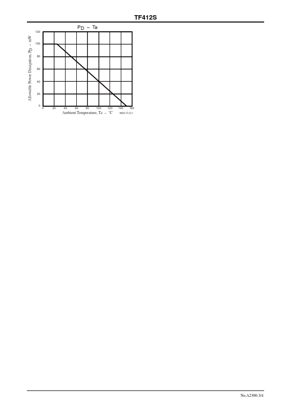
at Ta = 25C Parameter Drain-to-Source Voltage Gate-to-Drain Voltage Gate Current Drain Current Power Dissipation Junction Temperature Symbol VDSX VGDS IG ID PD Tj Value 30 30 10 10 100 150 Storage Temperature Tstg 55 to +150 This product is designed to “ESD immunity < 200V*”, so please take care when handling. * Machine Model Unit V V mA mA mW C C Marking 31 2 SOT-883 A2 M M = Date Code Ordering & Package Information Device TF412ST5G Pb-free and Halogen Free Package SOT-883 Shipping 8,000 pcs. / reel Stresses exceeding those listed in theMAXIMUM RATINGS
table may damage the device.