onsemi TIP2955
PNP Silicon Power Transistors
| Part No. | TIP2955 |
|---|---|
| Datasheet | TIP2955 Download |
| Manufacturer |  onsemi |
| Description | PNP Silicon Power Transistors |
| Buy | Stock & Price |

FEATURES
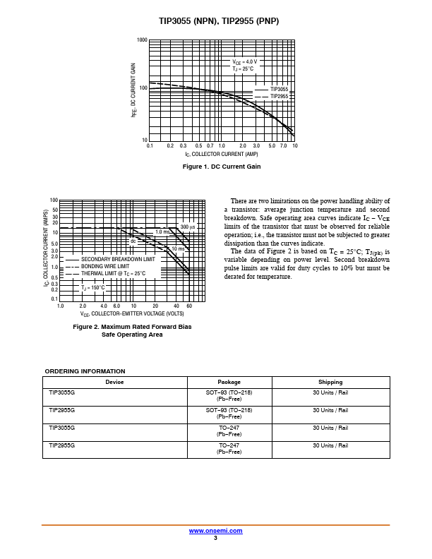
● DC Current Gain − hFE = 20 − 70 @ IC = 4.0 Adc● Collector−Emitter Saturation Voltage − VCE(sat) = 1.1 Vdc (Max) @ IC = 4.0 Adc
● Excellent Safe Operating Area
● These are Pb−Free Devices*
MAXIMUM RATINGS
Symbol Rating Value Unit VCEO VCER VCB VEB IC IB PD Collector − Emitter Voltage Collector − Emitter Voltage Collector − Base Voltage Emitter − Base Voltage Collector Current − Continuous Base Current Total Power Dissipation @ TC = 25°C Derate above 25°C 60 Vdc 70 Vdc 100 Vdc 7.0 Vdc 15 Adc 7.0 Adc 90 W 0.72 W/°C TJ, Tstg Operating and Storage Junction Temperature Range – 65 to °C + 150 Stresses exceeding those listed in theMAXIMUM RATINGS
table may damage the device. If any of these limits are exceeded, device functionality should not be assumed, damage may occur and reliability may be affected. THERMAL CHARACTERISTICS Symbol Characteristic Max Unit RqJC RqJA Thermal Resistance, Junction−to−Case Thermal Resistance, Junction−to−Ambient 1.39 35.7 °C/W °C/W *For additional information on our Pb−Free strategy and soldering details, please download the onsemi Soldering and Mounting Techniques Reference Manual, SOLDERRM/D.