QPB9325
QPB9325 is High Power Switch LNA Module manufactured by qorvo.
®
High Power Switch LNA Module
Product Overview
The Qorvo® QPB9325 is a highly integrated front-end module targeted for TDD macro or picocell base stations. The LNA switch module integrates RF functional blocks such as a pin-diode based high power switch capable of handling up to 52 W with an LTE signal (8 d B PAR) along with two LNA stages. Further integration is also implemented where the pin diode driver and dc-dc converter circuits are implemented inside the module to enable only the need for an external 5 V power supply. The control voltage for the switch and gain control. mode is with 3.3 V logic.
The QPB9325 can be utilized across the 3.6-3.8 GHz range to provide 1.2 d B noise figure for operation in the receive mode and 0.5 d B insertion loss in the transmit mode. The LNAs utilize Qorvo’s high performance E-p HEMT process while the switch allows for power levels up to 360 W peak power to be routed to an external load termination.
The QPB9325 is packaged in a Ro HS-pliant, pact 8x8 mm surface-mount leadless package. The switch LNA module is targeted for wireless infrastructure applications configured for TDD-based architectures.
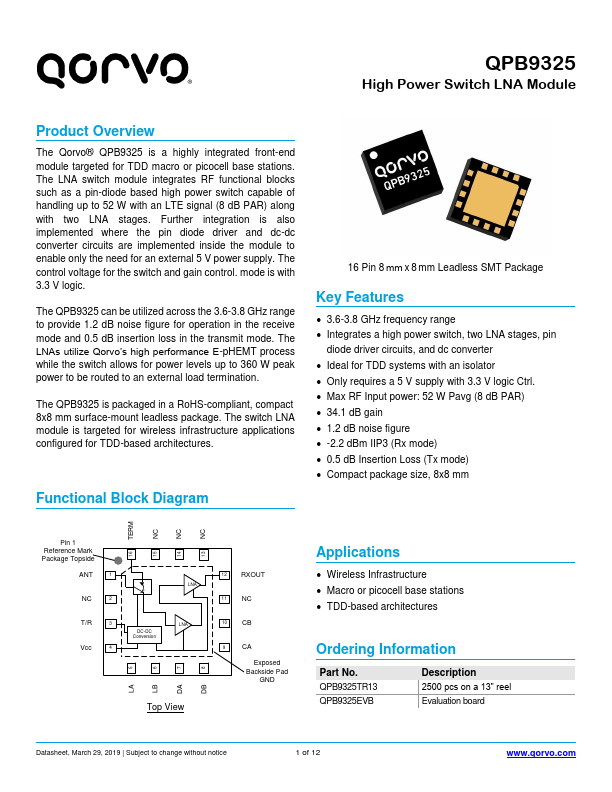
Functional Block Diagram
16 Pin 8 mm x 8 mm Leadless SMT Package
Key Features
- 3.6-3.8 GHz frequency range
- Integrates a high power switch, two LNA stages, pin diode driver circuits, and dc converter
- Ideal for TDD systems with an isolator
- Only requires a 5 V supply with 3.3 V logic Ctrl.
- Max RF Input power: 52 W Pavg (8 d B PAR)
- 34.1 d B gain
- 1.2 d B noise figure
- -2.2 d Bm IIP3 (Rx mode)
- 0.5 d B Insertion Loss (Tx mode)
- pact package size, 8x8 mm
16 TERM 15 NC 14 NC 13 NC
Pin 1 Reference Mark Package Topside
T/R
Vcc
DC-DC Conversion
LNA LNA
DA 7
Top View
12 RXOUT
Exposed Backside Pad
Applications...